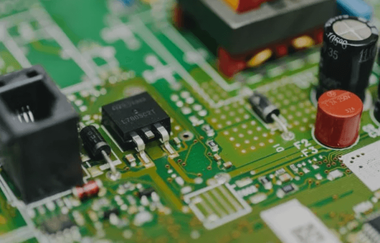
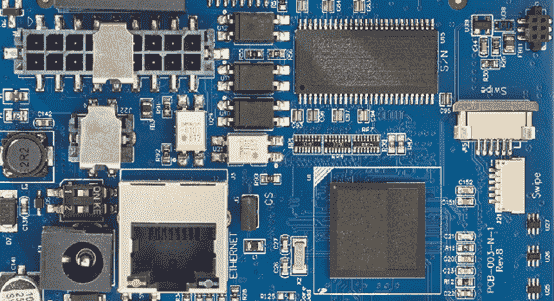
PCBs are used in a wide range of electronic devices, including computers, smartphones, and other digital equipment. They have become ubiquitous because they offer high reliability at a low cost. However, there are many different ways to treat the surface of a PCB before it is assembled with other components into an electronic device. Which…
カテゴリーアーカイブ: News
08
9月
9月
Many customers due to the lack of understanding of the PCB lamination pressing process, have suffered a lot of losses: get the multi-layer board but found warping, stratification is obvious, and even the existence of serious quality problems such as the open circuit of the inner layer. The main reason is that some factories do…
01
9月
9月
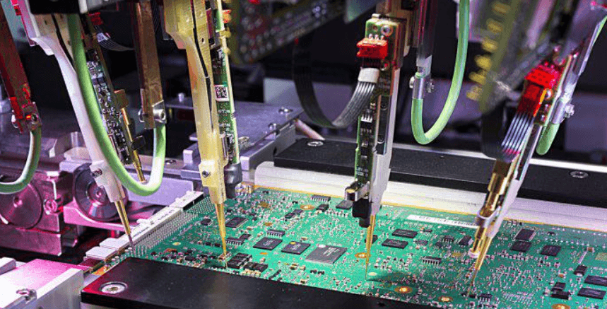
General PCB production will do the full inspection after the completion of two steps: one is the completion of the circuit (inner layer and outer layer); The second is after the finished product. The way to check the circuit after the inner and outer layer The electrical measurement method is one of the stress testing…
09
4月
4月
After we finished PCB design, send it to the PCB factory for PCB prototyping or mass production, will enclose a copy of the PCB process document, one is to indicate the PCB surface finishes, and different PCB surface finishes, their cost, and the application situation is different. Firstly, why do we need special treatment of…
31
マー
マー
Problem Cause Effect LNA/tank circuit arrangement (receiver) Inductor orientation RF feedthrough Degeneration/π-network arrangement (transmitter) Inductor orientation RF feedthrough Shared ground vias between legs of π network Via parasitics Feedthrough, RF leakage Shared ground vias between receiver blocks Via parasitics Crosstalk, RF feedthrough, RF leakage Long traces for decoupling capacitors Higher-impedance connections Reduced decoupling Wide component…
29
マー
マー
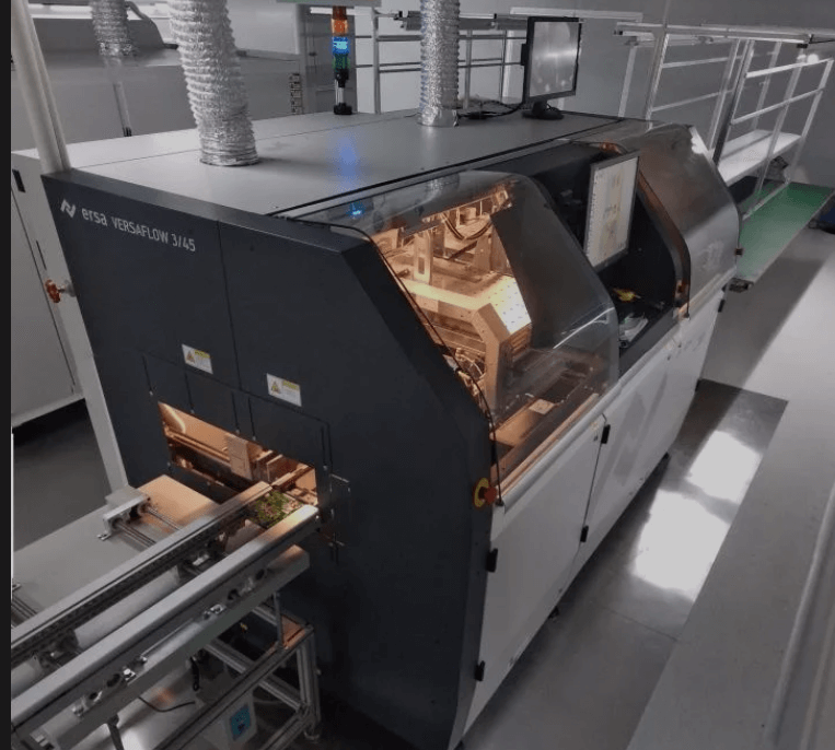
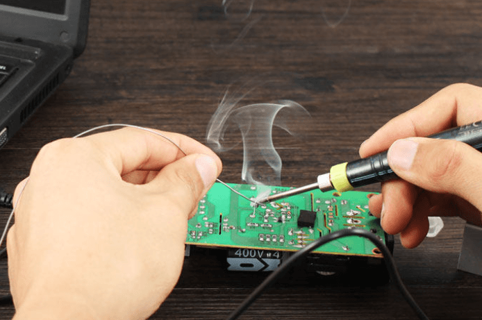
Introduction to wave soldering technology DIP plug-in and SMD adhesive process special wave soldering is one of the important processes of modern electronic manufacturing in PCB assembly industry, although it has been affected by SMT technology, but there are still quite a lot of electronic components can not be completely replaced by SMT packaging technology,…
24
マー
マー
Nowadays, the demand for electronic PCBA hardware terminal customers for electronic contract manufacturing services is increasingly strong. The traditional PCBA manufacturers, due to weak supply capacity, lack of price advantage, unstable supply, and low labor efficiency, lead to low conversion rate and face the problems of fewer and fewer customers. However, in the process of…
23
マー
マー
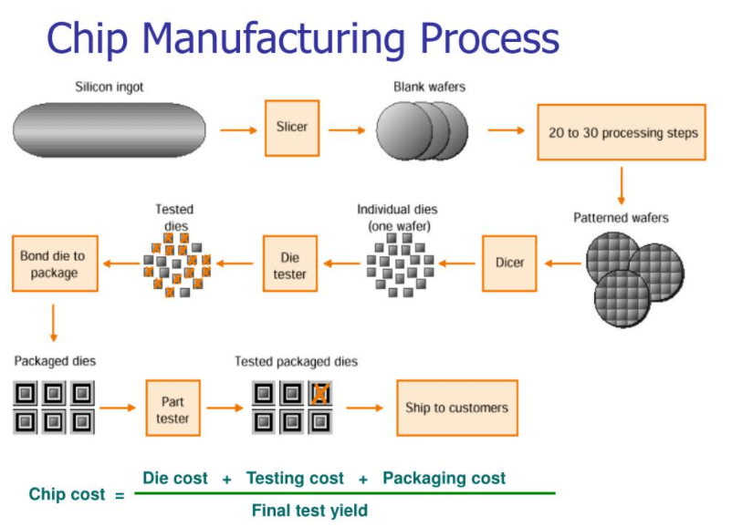
IoT chip to the module, the whole process of R&D and production The development of the Internet of Things and smart home has deepened the connection and interaction between people and things, making our lives more colourful, more convenient and more closely connected. The connection of people and things (equipment) depends on the Internet wireless…
18
マー
マー
what is a printed circuit board? The structure and characteristics of commonly used copper clad laminates Copper clad phenolic paper laminate A laminate made of insulating impregnated paper (TFS-62) or cotton fibre impregnated paper (1TZ-63) impregnated with phenolic resin and then hot pressed. In conclusion, with a single sheet of alkali-free glass impregnated cloth that…
16
マー
マー
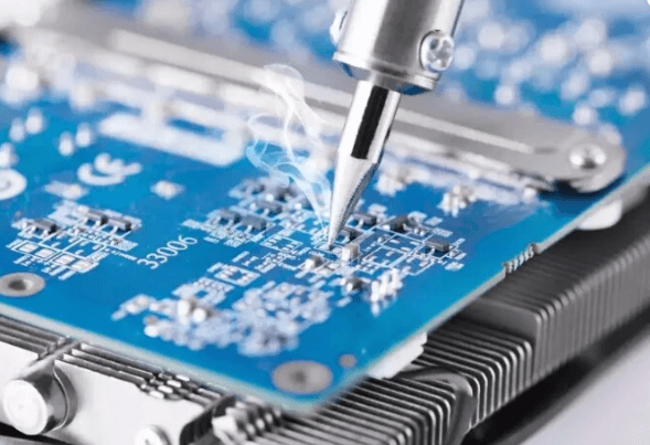
For decades, printed circuit board assembly (PCBA) has successfully developed in a stable manner. It is a key component of various machines, computing terminals, automobiles and other electronic equipment. It is compact and efficient. In addition, they electronically introduce new inventions and technologies on a global scale. They have set off an innovation in the…