This article explains what a chip on board is, how manufacturers construct it, and its different applications. Learn more about this cost-saving, protective, and efficient manufacturing process.
Introduction
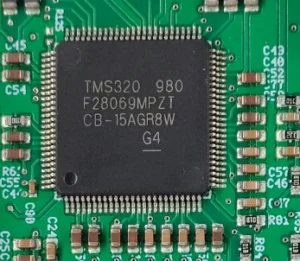
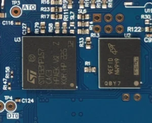
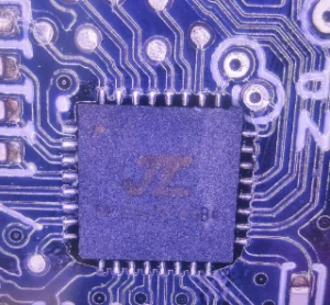
Upon opening an electronic assembly, you probably saw a strange-looking blob on a circuit board. It may look peculiar initially, as it appears to have gone out of shape. However, upon testing, you see that the blob does its intended application. This strange circuit assembly has a Chip on Board (or COB for short) inside.
What is a Chip on Board?
As its name implies, a chip-on-board is a chip assembly on top of a PCB. A COB comprises an integrated circuit (on a die or silicon wafer slice) wire-bonded or soldered through pads on the circuit board. After bonding or welding, a machine injects epoxy or plastic coating. This coating protects the sensitive die and wire bonds from moisture. It also shields them from mechanical and electrical stresses.
History of Chip on Boards
Electronics manufacturers developed chip-on-boards (COBs) to reduce manufacturing costs. They eliminated the need for integrated circuit packaging and saved space on circuit layouts. You’ll usually find COBs on cheap electronic goods (such as calculators, LCDs, electronic toys, and the like). You can also find COBs in areas like LED lighting and radio-frequency applications. They are also used in miniaturized electronic products, such as mobile phones and smart cards.
COBs are great for LED lighting. This is because LED chips can be crammed together on a board in a single LED package (as you’ll see later). Also, COBs have good thermal and power-efficient traits. These traits are useful for the said application.
COBs can benefit RF electronic circuits since a COB assembly eliminates the need for a lead frame, resulting in shorter lead lengths. This feature improves a circuit’s capacitive and inductive properties. It is great for RF circuits.
Nowadays, manufacturers employ COBs extensively since the trend of miniaturizing electronic products continues. As a result, more PCB fabrication houses may offer COB manufacturing. It’s best to contact them about their COB manufacturing capabilities.
How is a Chip on Board Constructed?

Several steps are involved in making a COB. You’ll need to know how to handle and wire-bond a chip die for wire-bonded COBs. You’ll also need to prepare some chemical materials to place the die and encapsulate the integrated circuit assembly. Here are the steps:
1. The fabricator manufactures the printed circuit board with pads ready to receive a chip die or wafer slice. The designer should calculate the spacing of these pads so that they can be wire-bonded on the chip die quickly and reliably.
2. The PCB is cleaned and prepared to receive the chip die. The die lands in the PCB substrate part, where a thin layer of adhesive material is applied to hold it in place.
3. The chip die is handled and placed on the exposed substrate with adhesive material on the PCB. The operator should carefully align these dies with a die-attach. They attach to the exposed copper pads on the substrate’s surface for wire bonding.
4. A wire bonding machine bonds the die pads to the patterns of the PCBs exposed pads. The PCB pads must withstand the heat of the wire bonding process. With this, the pads should be designed with a gold finish or have thicker copper tracks.
5. We apply an encapsulating material, usually epoxy, to the assembly’s surface. It protects the sensitive parts (the die, PCB pads, and wire bond assembly) from the environment. This part is the black blob you see primarily on top of the circuit board.
Some Variants of Chip on Boards
There are different variants of COBs, and they have their own advantages and particular applications.
1. Flip-Chip COBs
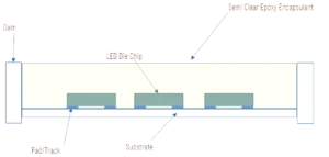
Flip-Chip COBs have dies placed with die-attach pads under the substrate. That’s where the term comes from; they look like inverted chips when assembled. This configuration uses a BGA-type connection to connect to their PCB substrates. This setup means they have solder bumps underneath them. The encapsulant is usually along the solder joints and below the die, which is called an underfill. Operators do not need to put wire bonds on the top dies. So, COBs for LED applications are much brighter than wire-bonded non-flip-chip COBs. LED manufacturers use Flip-chip COBs so that surface-mount LED chip dies have tighter spaces between them. This configuration produces a somewhat singular light source effect.
Flip-chip LED dies usually connect with other flip-chip LEDs to form a series circuit. The ends of this circuit connect to electrical pads on the substrate, reducing the number of pads on LED packaging. The number of LEDs crammed on a substrate determines the brightness level an LED package can offer.
2. Wire-bonded COBs
a. Wire-Bonded COBs (for LEDs)
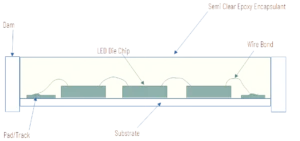
Like the Flip-Chip, manufacturers employ Wire-Bonded COBs for LED applications. Inside some high-power surface-mounted LEDs, you’ll see a Wire-Bonded COB configuration. A gold wire bond connected from the top die-attach to its corresponding electrical connection on the substrate should be seen. This kind of assembly makes LEDs electrically and thermally efficient. However, Flip-chip COBs are more efficient. They are better electrically and thermally. This is because they lack the wire bonds that can cause power loss.
Like flip-chip LEDs, wire-bonded LEDs can also connect in series. This forms a series circuit, reducing the number of pads in an LED package while making them brighter. However, flip-chips have an added advantage as they don’t need the wire bonds.
b. Wire-bonded COBs with encapsulation

Wire-bonded COBs have their top die-attach wire bonded to the exposed pads of a PCB. After this, the manufacturer encapsulates it in an epoxy coating as protection. You’ll find this configuration on many cheap electronic products, such as calculators, toys, and LCD modules. Wire-bonded COBs are inexpensive to make in volume compared to their IC-packaged counterparts. You can also save space on your projects in this type of configuration. Also, you can use encapsulation to make your component sturdier. It will also make it thermally efficient and protected.
Some Encapsulation Techniques on COBs
The COB assembly is fragile; the die and wire bonds are sensitive to physical stress. Additionally, moisture and other compounds can affect the parts of the COB, degrading it over time. Because of this, encapsulation techniques are employed to protect the assembly. Below are the usual encapsulation methods.
1. Glob Top Dispensing
This encapsulation technique uses an epoxy (or a type of UV-curable) compound that protects the whole COB assembly when it dries. The compound is applied through a narrow needle valve and allowed to flow over the entire COB. Measuring the compound’s viscosity is essential to ensure it won’t damage any wire bond during encapsulation. Also, an operator should watch the amount of compound dispensed. This prevents the COB’s height from reaching the allowed limits.
Glob-top encapsulation can insulate the COB. It also protects it from dangerous chemicals and moisture. This technique can also support the entire COB structure. It does so from mechanical stresses during handling.
2. Dam and Fill Dispensing
Dam and Fill dispensing uses two kinds of viscosity materials. The first is a high-viscosity material that creates a dam on the sides of the COB, and the second is a lower-viscosity material on the inside of the dam.
The higher-viscosity material limits the flow of the lower-viscosity material. It does so outside the areas protected by the dam. After this, the fabricator dispenses the lower-viscosity material at higher speeds compared to the higher-viscosity material.
This dispensing technique is faster than the glob top technique. It makes a better, uniform structure. The structure is predictable and has a tighter tolerance. Because of the said properties, dam and fill dispensing is used more on low-profile electronics.
Different Applications for Chip on Boards
Manufacturers can use chip-on boards in multiple applications. Below are some examples.
1. Lighting Applications
COBs’ power and thermal efficiency characteristics make them well-suited for LED lighting applications. Wire-bonded COBs have very short wire bonds that are superior conductors of electricity. Examples of these wires are gold, aluminum, copper, and silver. Flip-chip COBs are better because they don’t use wire bonds and can electrically attach to pads or tracks directly through solder bumps.
2. RF circuits
COBs are better for RF circuits. These circuits are affected by the inductive and capacitive properties of materials. They do this through very short electrical connections. COBs eliminate the leadframe and package of an IC. The die connects to the circuit pads/tracks through wire bonds or BGA-like solder bumps.
3. Cheap Integrated Circuits
As mentioned before, manufacturers widely use COBs for cheap electronic goods. These items benefit from the cost reductions of using integrated circuits with no packaging. Initial setup costs exist in manufacturing. But, they are overshadowed by the huge number of products made through mass production.
4. Aerospace Engineering

COB can become reliable and durable over time. It can then withstand tough conditions. This condition is perfect for aerospace. They need components with low failure rates for a long time.
The compact nature of COBs helps with space-constrained designs crucial for aerospace engineering. For example, designers can apply COBs to circuits. The circuits are embedded in boards crammed into different modules in a space-conscious space shuttle.
Operators can subject Aerospace components to high thermal stress. A high-end embedded computing device is an example. Anodized aluminum can be applied to COB encapsulation to improve overall thermal conductivity.
Conclusion
COB manufacturing is a cost-and space-saving process. It can help most electronics design companies. This article discussed COB’s history, construction, various encapsulation techniques, and varied applications.