
שני מאפיינים חשובים של ייצור מעגלים מודפסים הם איכות ועלות. בימים הראשונים, היה כמעט בלתי אפשרי להשיג את שני המאפיינים. הכנסת האוטומציה בייצור מעגלים מודפסים בשנות ה-1950 וה-60 סללה את הדרך לאיכות עקבית ולהפחתת עלויות של מעגלים מודפסים בייצור המוני.
UET PCB היא יצרנית מנוסה של מכלולי PCB. החברה מחויבת לשמירה על איכות עקבית תוך שמירה על עלויות סבירות.
מבט קצר על איכות וחיסכון בעלויות בתהליך הרכבת המעגלים המודפסים (PCB)
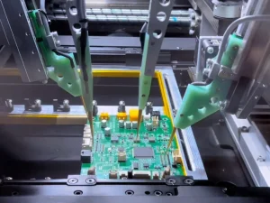
יצרנים השיגו חיסכון גדול עוד יותר בעלויות כאשר הוצגו טכנולוגיות רב-שכבתיות ו-SMT בשנות ה-1980. תהליכים אלה אפשרו גורמי צורה קטנים יותר של PCB עם צפיפות חיווט גבוהה יותר.
בתחילת המילניום החדש (2000), יצרנים ממזרח אסיה, ובמיוחד יצרנים סינים, השיגו חיסכון גדול אף יותר בעלויות. ממשלתם תמכה בהם בסובסידיות, מה שהפך אותם למרכז ייצור עולמי. כתוצאה מכך, חברות זרות רבות הקימו חברות ייצור מרוחקות בסין.
ישנן מספר אסטרטגיות ושלבים מרכזיים בייצור PCB איכותי. עם זאת, ישנם גם שלבים מרכזיים בהפיכת ה-PCBs לזולים יותר.
תהליך תכנון PCB לאיכות וחיסכון בעלויות
בחר גודל לוח סטנדרטי
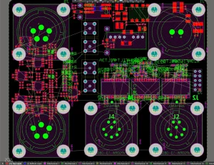
גודל לוח סטנדרטי יכול לעזור ליצרני PCB להפוך את תהליך הייצור לאוטומטי בצורה יעילה יותר. אם תשימו לב, גם גדלי לוח סטנדרטיים וגם גדלי לוח מינימליים חוסכים את התהליך. עדיף לחשב מראש גם את תקציבי הזמן וגם את תקציבי העלות אם אתם רוצים לייצר גודל לוח לא סטנדרטי.
בחר ערימה של לוח כלכלי
בחרו במערכת לוחות חסכונית לחיסכון משמעותי בעלויות. בדרך כלל, הוספת שכבות PCB נוספות פירושה קבלת לוח יקר יותר. לוח PCB דו-צדדי רב-שכבתי מדגם FR4 יכול להציע חיסכון משמעותי בעלויות מכיוון שקל יותר לייצר אותו ותהליך הלמינציה פשוט הרבה יותר. אם תבחרו ב-4, 6 או יותר שכבות, הכינו את עצמכם לחישוב העלות מראש לפני שתמשיכו בפרויקט שלכם.
מיקום רכיבים חוסכי מקום
לפני החיווט, מיקום רכיבים מתוכנן היטב יהפוך את הפריסה לקלה ומהירה יותר לביצוע. שיטה זו יכולה לחסוך זמן הנדסי משמעותי. בנוסף, שמירה על יישור אחיד של הרכיבים יכולה לעזור למכונת ה-Pick-and-Place להשלים את משימתה מהר יותר. שמירה על רכיבים בשכבה אחת (עליון או תחתון) תמיד תשמור על עלויות הרכבה נמוכות.
פריסת PCB לחיסכון במקום
פריסת PCB מקצועית צריכה להיות אופטימלית עבור שטח. רוב המסלולים צריכים להיות בעלי הנתיב הקצר ביותר. אי ביצוע פעולה זו עלול להאריך את החיווט, ובכך לבזבז שטח יקר על הלוח.
בחר דרך כלכלית
בחירה בטכנולוגיית ויה חסכונית יכולה להעניק לכם חיסכון משמעותי בעלויות. ויות סטנדרטיות ומוכחות הן תמיד אופציה טובה. עם זאת, בהשוואה לטכנולוגיות ויה יקרות יותר כמו מיקרו-ויות, ויות קדוחות לייזר, ויות עיוורות או ויות קבורות, ויות לחור בדרך כלל תופסות שטח גדול יותר. בהתחשב בכך, חשוב ליישם טכניקות ניתוב יעילות.
תהליך רכישת רכיבים לאיכות וחיסכון בעלויות
תחום נוסף לחיסכון בעלויות תוך שאיפה לאיכות הוא מיון קפדני של רכיבים. עליכם בהחלט לרכוש רכיבים ממפיצים/מקורות אמינים, אך יחד עם זאת, לקחת בחשבון את העלות. ישנן שתי שיטות לבחור מהן ברכישת הרכיבים שלכם:
| שיטת מקור רכיבים | מה זה | יתרונות חסרונות |
| Turn-Key | מתן אפשרות ליצרן ה-PCB שלך לבצע עבורך את איתור הרכיבים. | אספקה מהירה יותר של הפרויקט. חיסכון בעלויות עבור פרויקטים קטנים ובינוניים. |
| מִשׁגוֹר | אתה מקבל את הרכיבים בעצמך ואז שולח אותם ליצרן שלך | ייתכן שתיתקלו בעלויות לוגיסטיות, אם כי יש חיסכון משמעותי בעלויות בקנה מידה גדול. |
תהליך ייצור PCB לאיכות וחיסכון בעלויות
גימור משטח חסכוני
אם הפרויקט שלכם אינו דורש מחברים מיוחדים, רכיבים בעלי פסיעה עדינה או כבלי BGA, תוכלו לבחור בגימור פני השטח HASL המוכח. HASL הוא ראשי תיבות של Hot Air Solder Leveling. עם זאת, אם יש לכם צרכים מיוחדים, ייתכן שתצטרכו לבחור בסוגים האחרים. להלן טבלה שתוכלו לבדוק עבור גימורי פני השטח:
| גימור משטח | תמחיר | תיאור |
| HASL (פילוס הלחמה באוויר חם) | מאוד נמוך | עלול לייצר גימור לא אחיד, לא טוב ל-BGA או לרכיבים בעלי פסיעה דקה |
| OSP (חומר משמר יכולת הלחמה אורגני) | מעט גבוה | גימור אחיד, אך חיי מדף קצרים. טוב לסביבה. |
| טבילה בדיל / כסף | בינוני | גימור אחיד, טוב לצלחות עדינות כמו BGA, אך יכול להכתים בקלות. לכסף יש מוליכות טובה (טובה לתדר רדיו). |
| ENIG (זהב ניקל ללא אלקטרו) | גָבוֹהַ | גימור אחיד מאוד עם חיי מדף ארוכים. מתאים לצבעים עדינים כמו BGA. יכול ליצור אפקט של פד שחור. |
| ENEPIG | גבוה מאוד | זהה ל-ENIG אך מבטל את אפקט הרפידה השחורה. מוכן לחיבור חוטים. |
| זהב קשה | ממש גבוה | עמיד מאוד, מיועד לאנשי קשר בעלי אמינות גבוהה. אינו מתקלף. |
מסכת הלחמה חסכונית
יצרני PCB משתמשים בדרך כלל במסכת הלחמה נוזלית (LPI). עם זאת, הלקוח רשאי לבחור צבעים שונים לשם כך. האפשרות הסטנדרטית והמשתלמת ביותר היא ירוקה. עם זאת, ניתן לבחור צבעים אחרים בעלי עלויות וזמני גימור משתנים.
מסך משי סטנדרטי חסכוני
ייצור מודרני של PCB משתמש בדרך כלל בשיטת Liquid Photo Imaging (LPI) להדפסת משי. שיטה זו מדויקת וחסכונית כאחד. קיימת גם Direct Legend Printing (DLP), שהיא מדויקת יותר. עם זאת, שיטה זו יכולה לעלות לכם יותר.
סימונים מיוחדים
ייתכן שתמצאו סימונים מיוחדים או מספרים סידוריים במהלך ייצור המעגלים המודפסים. אלו הם מספרי בקרה עבור הלוחות שלכם. תוכלו לבחור להסירם, אם כי ייתכן שיהיה לכך עלות קטנה.
פאנליזציה של המעגלים המודפסים שלך
אם יש לכם מספר גדול של מעגלים מודפסים לייצר, ציפוי לוחות (PCBs) יכול להניב חיסכון משמעותי בעלויות. קל, מהיר וחסכוני יותר עבור יצרן לספק מערך לוחות מודפסים למכונת pick-and-place. תהליך פירוק הלוח המודפס הוא לרוב חסר משמעות עבור הלקוח הסופי.
תהליך בדיקת PCB
תהליך בדיקת ה-PCB יעזור לכם למיין לוחות שאינם מתפקדים או פגומים. הליך זה ימנע החזרות יקרות מצד הלקוחות. בחרו תמיד בבדיקה, במיוחד עבור לוחות המיוצרים בייצור המוני או מורכבים. להלן כמה מהליכי הבדיקה הידועים.
| תהליך הבדיקה | תמחור משוער | תיאור |
| AOI (פיקוח אופטי אוטומטי) | 0.01-0.05 דולר לפד | משתמש בציוד הגדלה גבוה כדי להסתכל על הלוחות |
| מבחן פונקציונלי | 50-200 דולר לג'יג | דורש ג'יג או הגדרה בהתאמה אישית שצוינו על ידי הלקוח |
| מבחן בדיקה מעופפת | 50-150 דולר למנה | בדיקה לאיתור פתח או קצרים במעגל מודפס. |
| צילום רנטגן | $30 - $80 לאצווה | מצא בעיות ב-BGA וב-ICs בעלי פסיעה עדינה |
| מיטת ציפורניים לתקשורת | 500-2000 דולר ליחידה
0.10-0.50 דולר ללוח |
בדיקות לייצור בקנה מידה גדול. חובה לכלול ג'יגים. |
סיכום
ישנן מספר אסטרטגיות להפחתת עלויות בייצור PCB שניתן ליישם מבלי להתפשר על האיכות. תהליכים אלה משתרעים על פני שלבים שונים של פיתוח הפרויקט, כולל תכנון PCB, איתור רכיבים, ייצור PCB ובדיקות. יעילות וידע טכני יכולים לעזור לשמור על עלויות הפרויקט נמוכות תוך שמירה על איכות.