For manufacturing companies, one of the main requirements for an order is its manufacturability. Unfortunately, in practice, we have to face a situation when the received order is not technological. This leads to an increase in the complexity of its manufacture, and, consequently, to an increase in cost. A similar situation can occur both in…
14
10月
10月
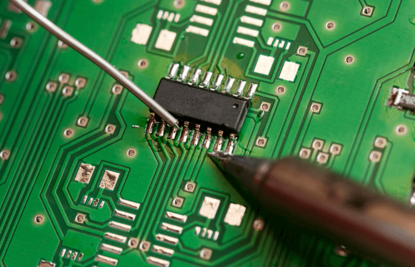
PCBs are a fundamental part of the design process in the electronic industry, and this article will provide you with an overview of what they are and how they differ from other types of circuit boards. PCBs can be utilized for prototyping, fabrication, and manufacturing purposes, but understanding all these pcb manufacturing process is important…
14
10月
10月
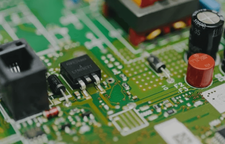
PCBs are used in a wide range of electronic devices, including computers, smartphones, and other digital equipment. They have become ubiquitous because they offer high reliability at a low cost. However, there are many different ways to treat the surface of a PCB before it is assembled with other components into an electronic device. Which…
08
9月
9月
Many customers due to the lack of understanding of the PCB lamination pressing process, have suffered a lot of losses: get the multi-layer board but found warping, stratification is obvious, and even the existence of serious quality problems such as the open circuit of the inner layer. The main reason is that some factories do…
01
9月
9月
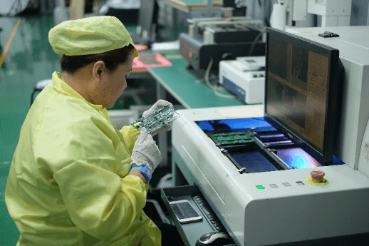
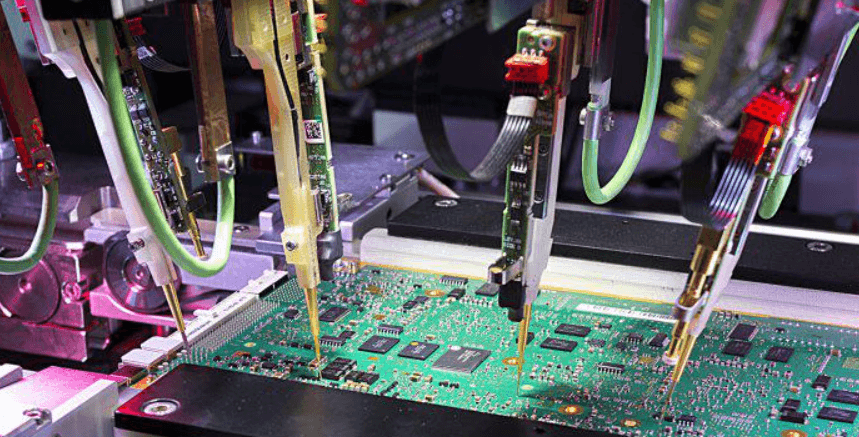
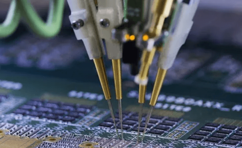
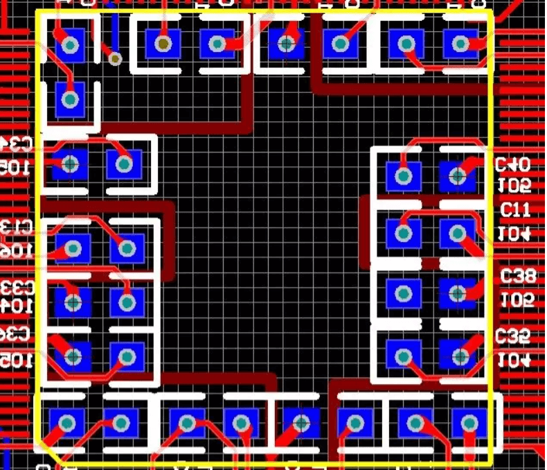
General PCB production will do the full inspection after the completion of two steps: one is the completion of the circuit (inner layer and outer layer); The second is after the finished product. The way to check the circuit after the inner and outer layer The electrical measurement method is one of the stress testing…
01
9月
9月
プリント回路基板(PCB)は、中国から最も輸出されている商品の一つである。この記事では、中国のプリント基板メーカートップ10を紹介する。電子機器のプリント基板製造に関しては、いくつかの選択肢がある。しかし、良いプリント回路基板は、良いデザインを得るための主な要因の一つです...
25
8月
8月
PCB電気テストについて知っておくべきこと なぜPCB製造中にPCB電気テストを始めるのか PCBボードの製造工程では、外的要因による短絡、開回路、漏電などの電気的欠陥を避けることは難しい。また、PCBは高密度化、微細化、高密度化へと進化を続けています。
18
8月
8月
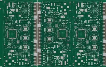
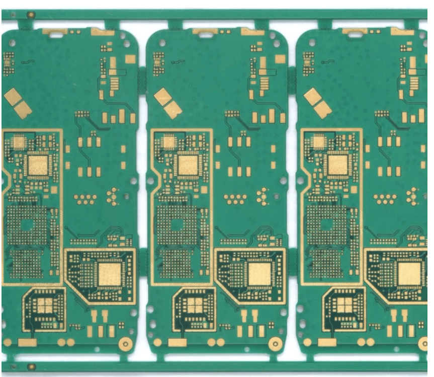
PCBAの生産効率を向上させ、生産コストを削減するために、通常、PCB回路基板は、PCBAのはんだ付けを容易にするだけでなく、時間を節約することができ、ボードアセンブリの生産のためにパネル化されます。PCBパネル化の目的は?SMTアセンブリの効率を向上させる。パネルに含まれる基板の数が多ければ多いほど、...
05
8月
8月
PCBバイアについて知っておくべきこと 回路基板は銅箔の層で構成されています。回路の異なる層は、穴(VIA)によって接続されています。回路基板の目的は電気を通すことなので、スルーホールと呼ばれます。PCBビアの種類 スルーホールのメッキ...
30
7月
7月
回路基板の製造は時間がかかる手順であり、「簡単なこと」とは思われていない。とはいえ、適切な材料があれば自宅で基板を自作できる愛好家もいるが、機械で作るものに比べると複雑さに欠ける傾向がある。また、時間もかかる。