
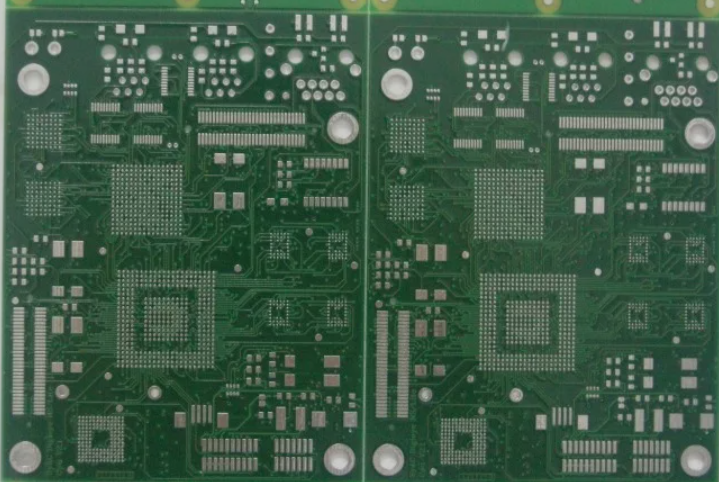
After we finished PCB design, send it to the PCB factory for PCB prototyping or mass production, will enclose a copy of the PCB process document, one is to indicate the PCB surface finishes, and different PCB surface finishes, their cost, and the application situation is different.
Firstly, why do we need special treatment of PCB surface?
Copper is easily oxidized in the air, and the oxidized copper layer has a great impact on PCB soldering. So it is easy to form false and bad solder, resulting in components that can not be well soldered. Therefore, we will have a process (pcb surface finish) in the PCB production to deal with these possible problems precisely. A special material is applied to the pads (plating) to protect the solder pads from oxidation.
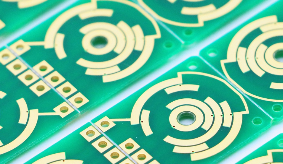
The PCB surface finishes have HASL with lead/lead-free, OSP, Immersion Gold (ENIG), Immersion Tin, Immersion Silver, Electroless Nickel Electroless Palladium Immersion Gold (ENEPIG), Hard Gold, and so on. Of course, there will be some special PCB surface finishes for special application occasions.
The advantages and disadvantages of different PCB surface finishes
1. Bare copper PCB
Copper surface finish advantages:
- Lower cost
- Flat surface
- Excellent solderability (in the case of no oxidation).
Copper surface finish disadvantages:
- Sensitive, easy to be affected by acid and humidity
- Short shelf life, needs to be soldered within 2 hours after unwrapping because copper exposure in the air is easy to oxidize.
- Cannot be used on double sides PCB, because the second side will be oxidized after the first side reflowing.
- If there are test points, the solder paste must be added on the test pads to prevent oxidation, otherwise subsequent contact with the probe will not be good.
2. HASL / Lead Free HASL(Hot Air Solder Levelling)
HASL pcb surface finish advantages:
- Lower price
- Good soldering performance
- Can repair
- Long shelf life.
HASL pcb surface finish disadvantages:
- Not suitable for fine pitch components and small components
- Uneven Surfaces,
- Thermal Shock
- Not good for HDI PCB.
It is easy to produce solder beads in PCB assembly process, which is easy to cause short circuits to fine pitch components. When used in double-sided PCB SMT process, because the second side has undergone a high-temperature reflow soldering, it is very easy to re-melt and produces solder beads or similar water beads into dropping spherical solder balls under the influence of gravity, resulting in an uneven surface, thus affecting the soldering.
The HASL pcb surface finishes technology do use to play a leading role in PCB surface finishes technology. In the past years, more than three-quarters of PCBs were HASL, but the industry has been reducing the use of HASL over the past decade. The HASL pcb surface finish process is dirty, smelly, and dangerous, so it has never been a favorite process, but it is excellent for larger components and wider-spaced lines.
In high-density PCB, the flatness of the HASL process will affect the subsequent assembly; Therefore, the HDI board generally does not use HASL as surface finish. With the development of technology, the industry has now appeared to be suitable for smaller assembly spacing of the QFP and BGA HASL process, but less practical use. At present, some factories use the OSP process and ENIG process to replace the HASL process.
The development of technology also makes some factories use immersion tin and immersion silver. Coupled with the trend of lead-free in recent years, the use of HASL pcb surface finish technology is further limited. Although there has been a lead-free HASL surface finish, this will involve equipment compatibility issues.
3. OSP (Organic Solderability Preservatives)
OSP pcb surface finish advantages:
- Flat Surface
- No Pb
- Simple Process
- Cost Effective
- Can repair that boards have expired (three months), but usually only once.
OSP pcb surface finish disadvantages:
- Short Shelf Life,
- Can’t measure the thickness
- Not good for PTH (Plated Through Holes)
- Sensitive and susceptible to acid and humidity.
Used in the second reflow soldering, need to be completed within a certain time. Usually, the second reflow soldering result will be poor. OSP is an insulating layer, so the test pads must be covered with solder paste to remove the original OSP before contacting the probe for an electrical test.
We can use OSP surface treatment for low-tech PCBs. It can also use for high-tech PCBs, such as single-sided TV PCBs and high-density chip package PCBs. For BGA, OSP uses widely. If there is no surface connection functional requirement or limiting of shelf life for PCB, the OSP process will be the most ideal surface finish. However, OSP is not suitable for a small number of diverse products and is not suitable for products with uncertain demand estimates. If the company’s inventory of printed circuit boards is often more than six months, it is not recommended to use OSP surface finish PCB boards.
4. ENIG (Electroless Nickel Immersion Gold)
Enig pcb surface finish advantages:
- Not easy to oxidize
- Long shelf life
- Flat surface
- No Pb
- Can repair
- Good conducting for PTH (Plated Through Holes)
- Suitable for fine pitch components and small components and components with small solder pads
- Preferred with keypad PCB board
- The ability to repeat reflow soldering multiple times does not necessarily reduce its solderability. Enig pcb surface finish can use as the base material of the COB (Chip On Board).
Enig pcb surface finish disadvantages
- More Expensive
- Poor soldering strength
- Easy to have the problem of Black Pad / Black Nickel, as using a nickel plating process.
Different from the OSP surface finish, the ENIG pcb surface finish is mainly used on PCB boards with functional surface connection requirements and long shelf life. Due to the flatness of the HASL process and the removal of the flux in the OSP process, ENIG was widely used. But because of the black pad that happened in the ENIG pcb surface finish, the application of ENIG technology has been reduced. Usually, portable electronic products (such as mobile phones), almost all use OSP, immersion tin, and immersion silver. And adopts ENIG to form as buttons area, contact area, and EMI shielding area, it is called selective ENIG pcb surface finish technology.
5. Immersion Silver (IAg)
Silver immersion pcb advantages:
- Cheaper than ENIGFlat surface
- Suitable for fine pitch components, small and BGA components
- Good solderability
- No Pb Can be repaired
Silver immersion pcb Disadvantages:
- Very sensitive to handling
- High storage conditions required
- It is easily contaminated, oxidized
The process of immersion silver is between ENIG and electroless nickel, which is simple and fast. Even when exposed to thermal and humidity environments, the silver retains good solderability but loses its luster. If PCB has connection function requirement and needs to reduce cost, immersion silver is a good choice.
With good flatness and contact, Silver immersion pcb use widely in communication, automotive, computer products, and high-speed signal design. Due to its good electrical properties, immersion silver can also be used in high-frequency signals. EMS recommends the immersion silver process because it is easy to assemble and has good inspection performance.
6. Immersion Tin (ISn)
Immersion tin pcb surface finish advantages:
- Flat surface No Pcb Repairable
- Good solderability
- Suitable for fine pitch components, small and BGA components
Immersion tin pcb surface finish disadvantages:
- After assembly process, it’s easy to expose Tin
- Not good for multiple reflow soldering
- Sensitive to handling Contains carcinogens
- It’s corrodible to solder mask
Immersion tin does not introduce any new elements in the soldering, so especially suitable for communication PCB board. Tin will lose its solderability beyond the shelf life of the board, so better storage conditions are needed for immersion tin. In addition, the immersion tin surface finish is limited to use due to the carcinogenic substance.
7. Electroless Nickel Electroless Palladium Immersion Gold (ENEPIG)
Advantages:
It can use in a wide range of applications. At the same time, ENEPIG surface finish can effectively prevent the connection reliability problems caused by black pad defects and can replace ENIG surface finish.
Disadvantages:
While ENEPIG has many advantages, Pd is expensive and a scarce resource. At the same time, the fabrication process control requirements are strict and complicated.
Compared with ENIG, ENEPIG has an extra layer of Pd between Ni and Au. In the deposition reaction of replacement Au, the electroless Pd coating protects the nickel layer from being overly corroded by the replacement Au. Pd is fully prepared for Au leaching while preventing corrosion caused by replacement reaction. The thickness of Ni is generally 120~240μin (about 3~6μm) and Pd is 4~20μin (about 0.1~0.5μm), The deposit thickness of Au is generally 1~4μin (0.02~0.1μm).