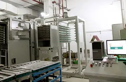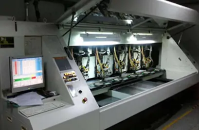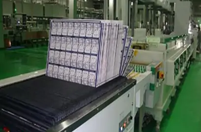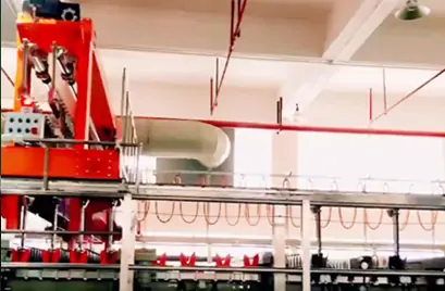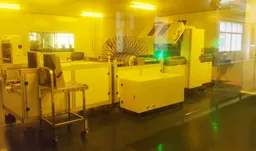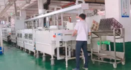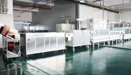
Pcb prototype service introduction
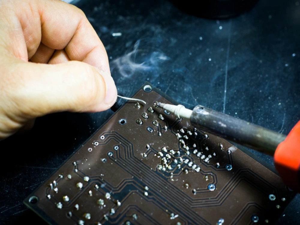
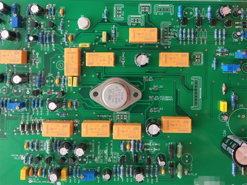
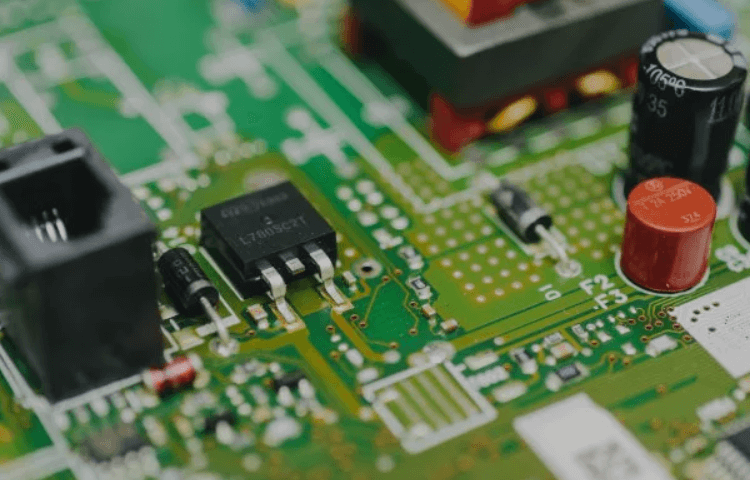
Component assembly
| Feature | Through-Hole | SMT (Surface Mount Technology) |
|---|---|---|
| Component Type | Long-leaded, larger components (e.g., electrolytic capacitors, transformers) | Compact, leadless components (e.g., SMD resistors, ICs) |
| PCB-ontwerp | Requires drilled holes (common for single/double-layer boards) | No drilling needed (ideal for high-density multilayer boards) |
| Mechanical Strength | High (suitable for physical stress or high-temperature environments) | Lower (relies on solder paste adhesion) |
| Cost/Efficiency | Higher labor costs (ideal for prototypes/low-volume) | Highly automated (optimized for mass production) |
Manual and automated Insertion
Lead-free or RoHS soldering
Double Wave Flow Solder
Selective wave soldering
Use low and high melting point solder
Conformal Coating
IC Programming
Inspection and functional testing
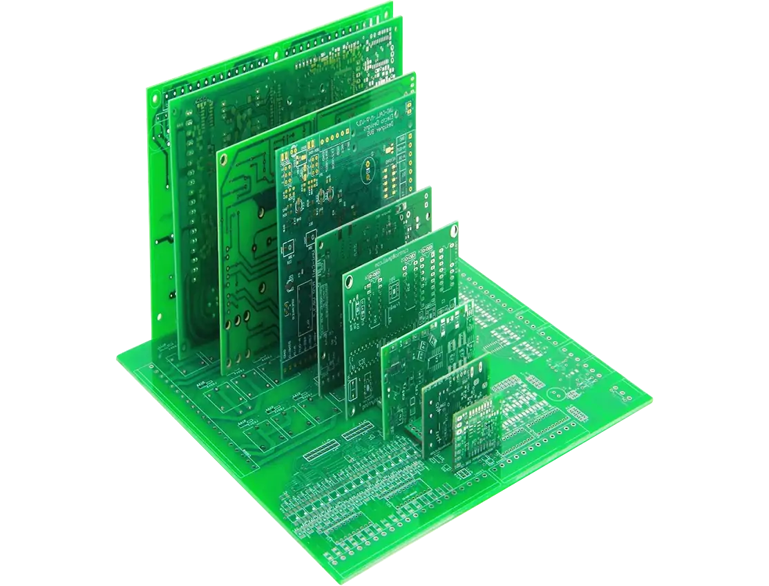
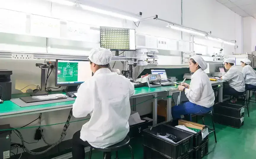
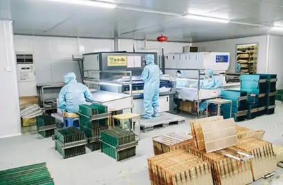
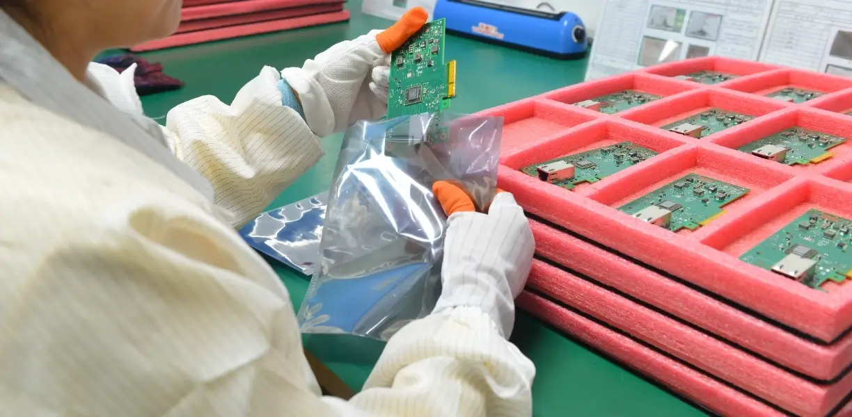
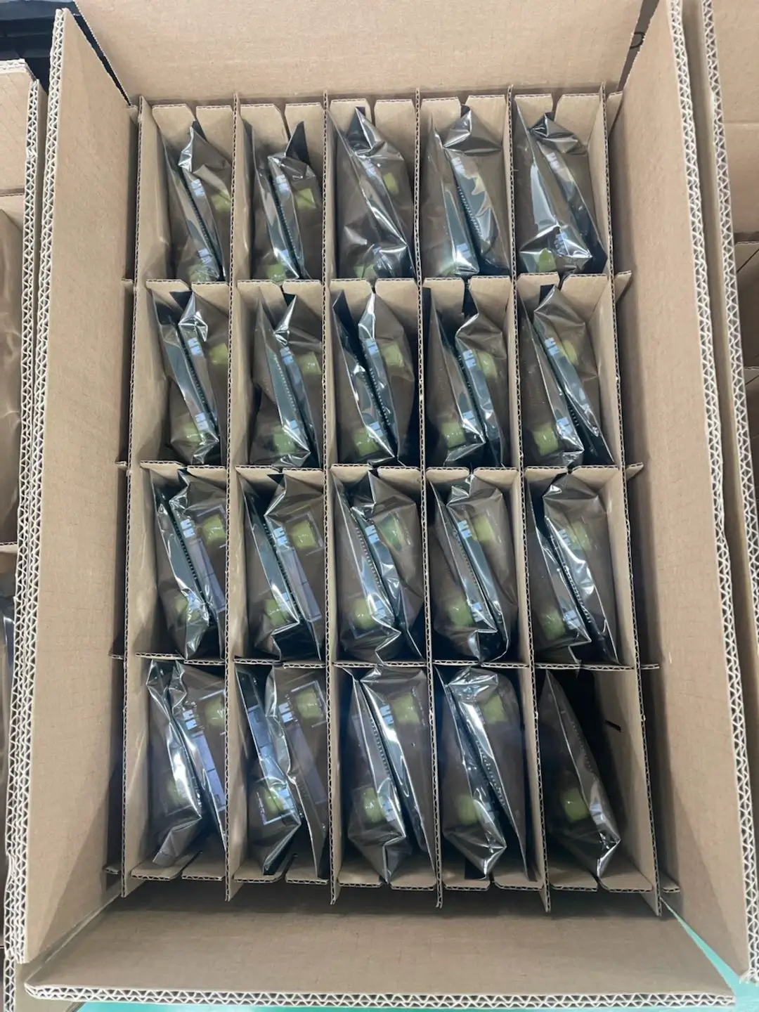
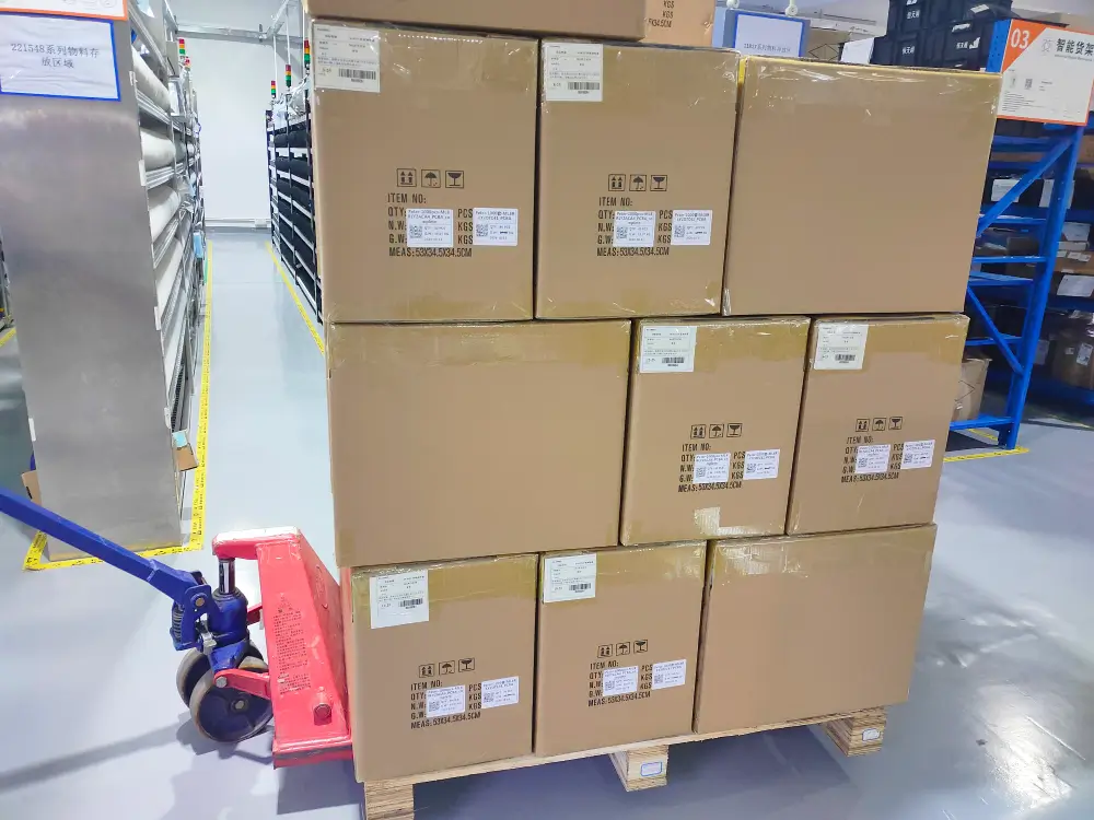
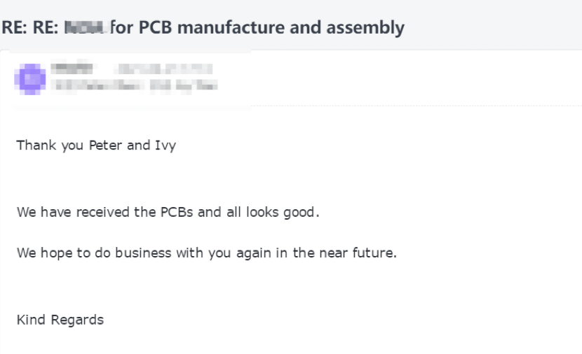
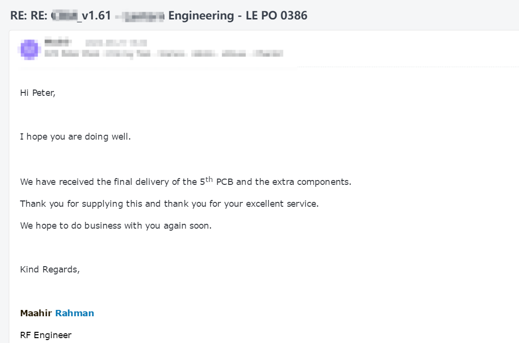
UETPCB is een professionele leverancier van printplaten en fabrikant van geassembleerde printplaten (PCBA) in Shenzhen. Wij richten ons op het leveren van hoogwaardige assemblagediensten voor printplaten. Als betrouwbare leverancier van printplaten bieden wij een totaaloplossing, van de productie van printplaten tot de assemblage ervan. Ons professionele team beschikt over de ervaring en vaardigheden om aan de behoeften van diverse sectoren te voldoen. Ons doel is om uw voorkeurspartner te zijn op het gebied van PCBA-productie in China. Neem gerust contact met ons op als u op zoek bent naar hoogwaardige printplaatassemblage.
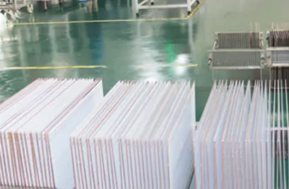
Step 1:Creating a designed layout on the copper-clad laminate
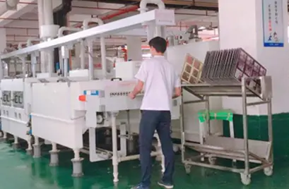
Step 2:PCB manufacturers will etch or remove excess material from inner layers to reveal images and pads.
Step 3:Laminating printed circuit board materials at high temperatures for creating the PCB layer stack up
Step 4:Creating mounting holes, through-hole pins, and vias on PCB
Step 5:Etching and removing the excess copper of the surface layer to reveal images and pads
Step 6:Placing plating pin holes and via holes
Step 7:Creating a protective coating or solder masking on the surface
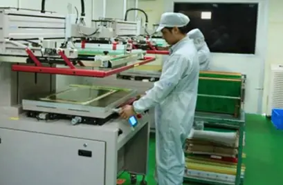
Step 7:Silkscreen printing, logos or other markings, and installing polarity indicators on the surface
Heeft u vragen? Neem gerust contact met ons op; wij beantwoorden uw vragen binnen 24 uur.
We specialize in building your pcb prototype and PCB assembly with rapid turn times.