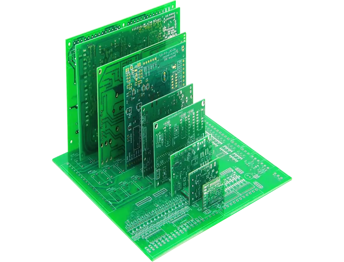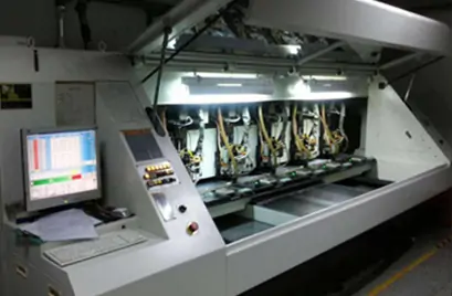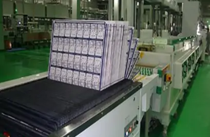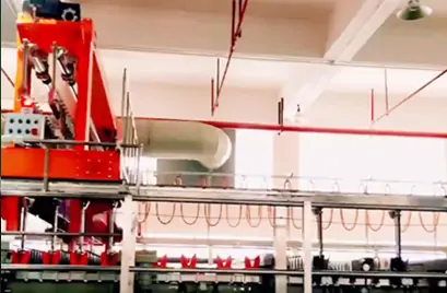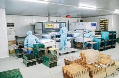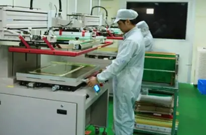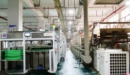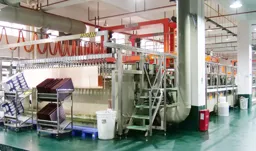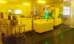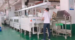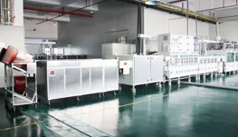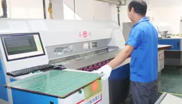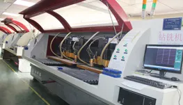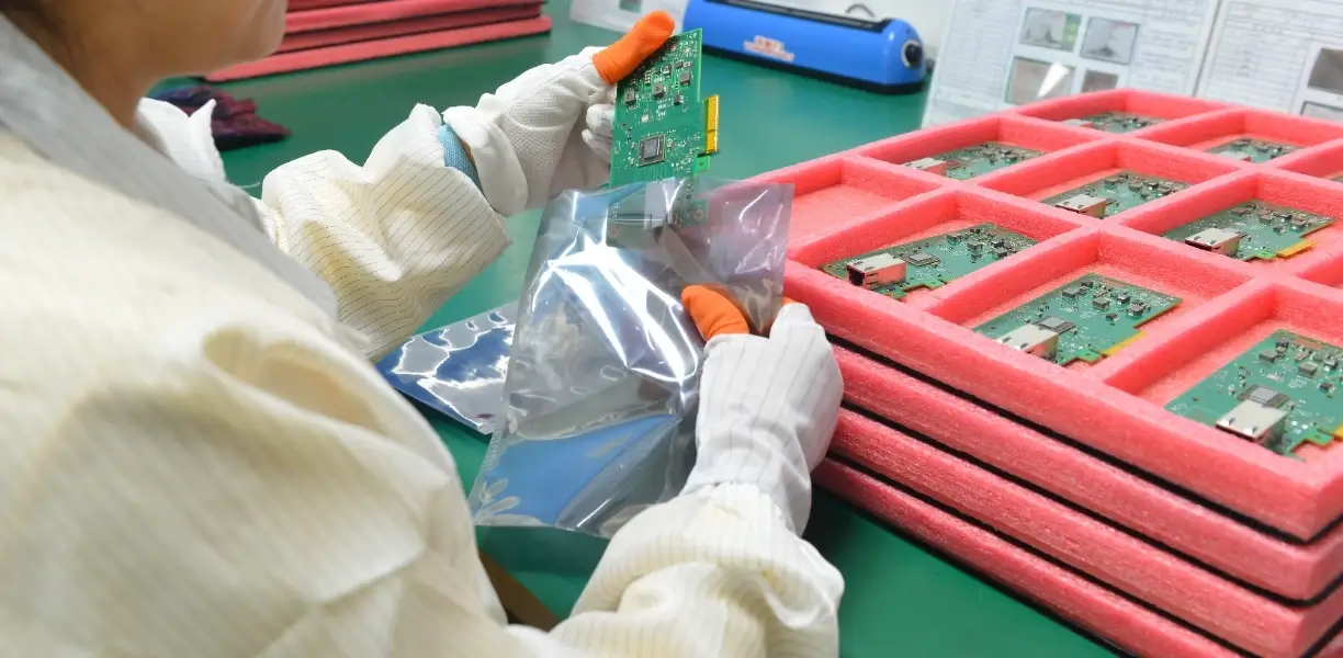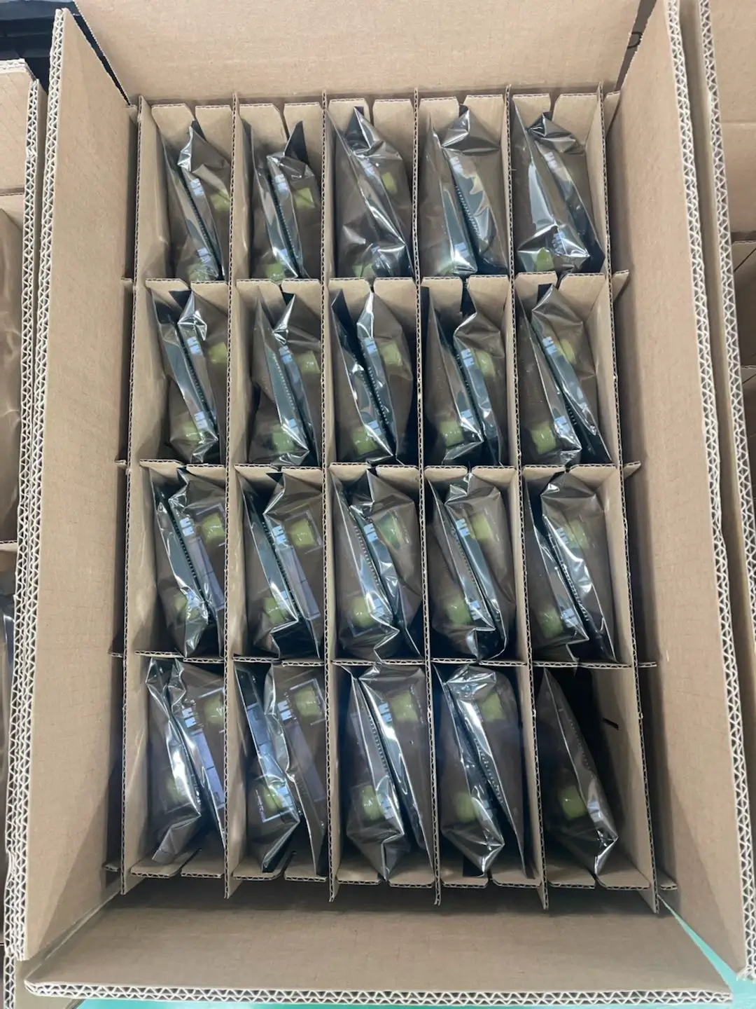
Pcb prototype service introduction
Component assembly
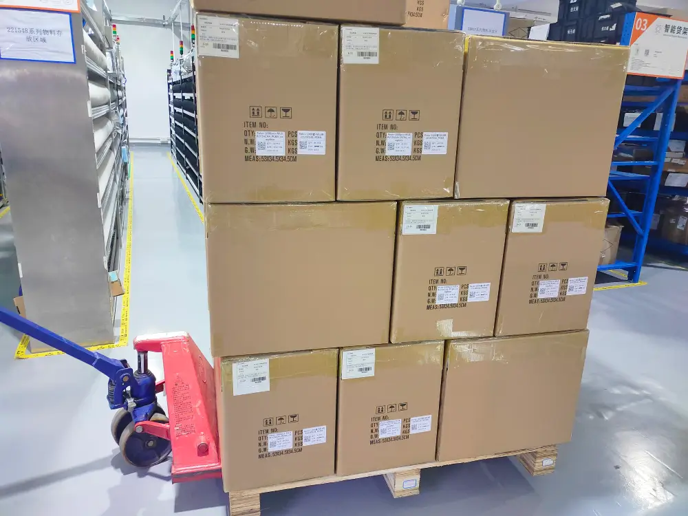
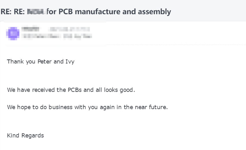
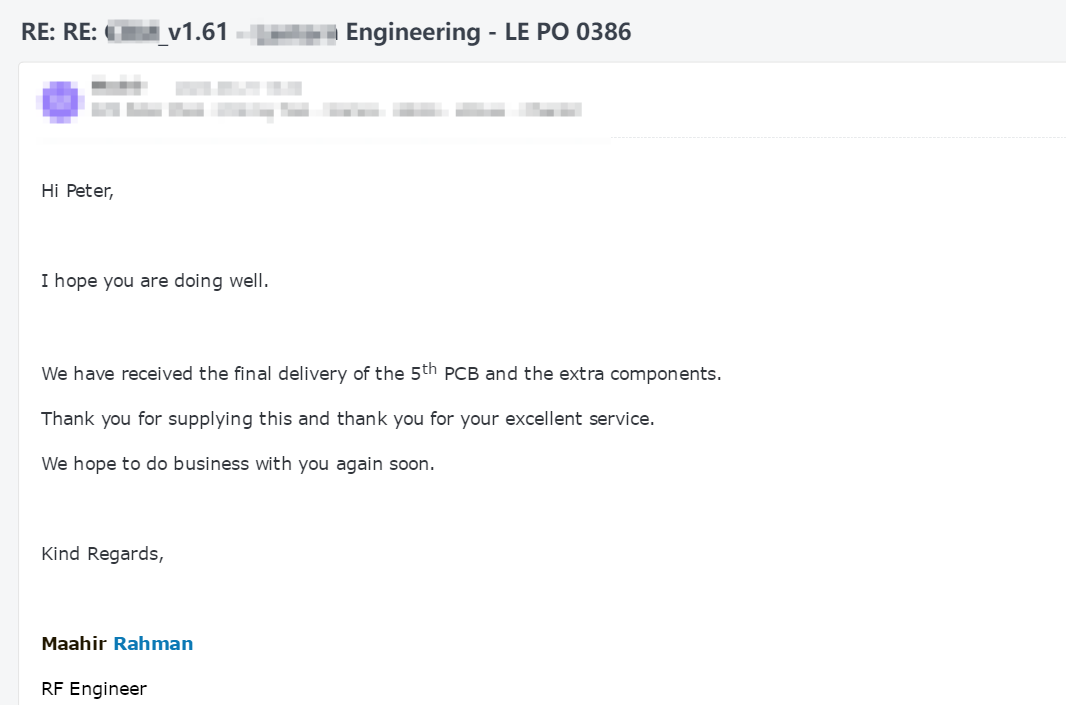
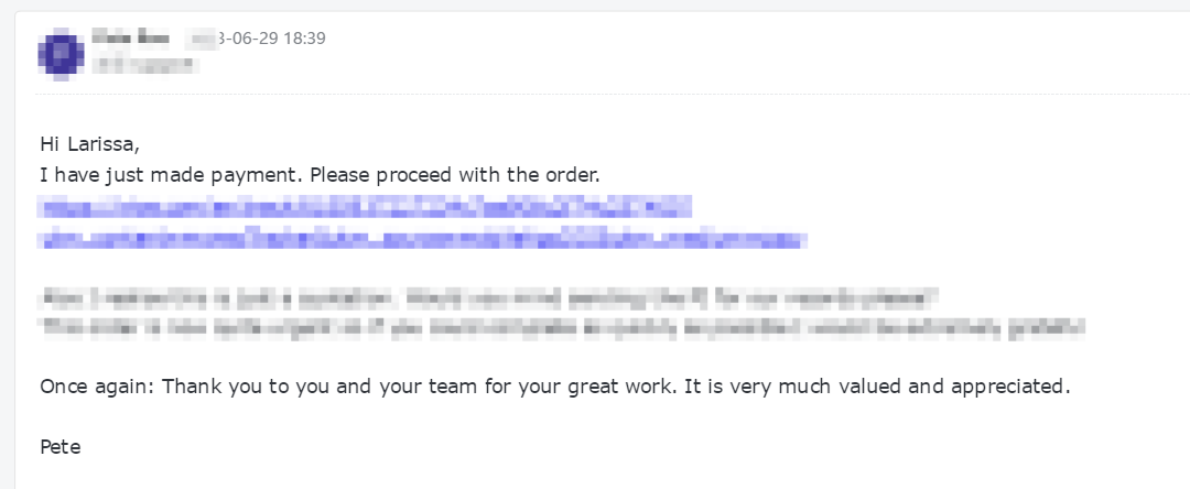
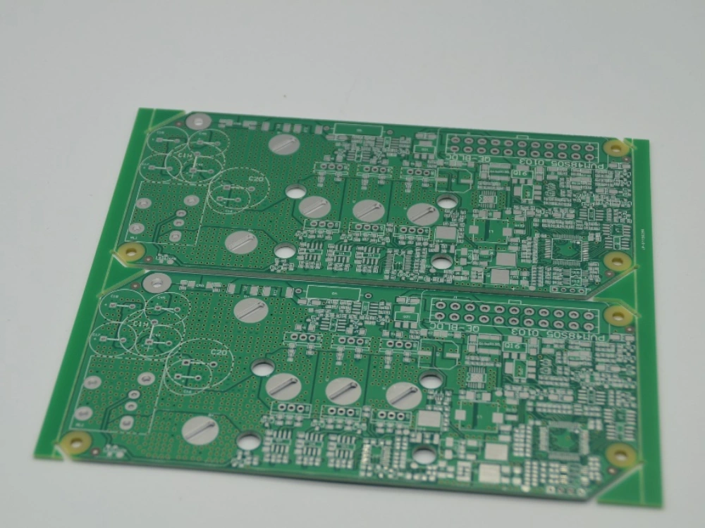
UETPCB — профессиональный поставщик печатных плат и производитель сборки печатных плат (PCBA) в Шэньчжэне. Мы специализируемся на предоставлении высококачественных услуг по сборке печатных плат. Являясь надежным поставщиком печатных плат, мы предлагаем комплексные услуги — от изготовления печатных плат до их сборки. Наша профессиональная команда обладает опытом и навыками, необходимыми для удовлетворения потребностей различных отраслей. Наша цель — стать вашим предпочтительным партнёром в сфере производства печатных плат с монтажом (PCBA) в Китае. Если вам нужны качественные услуги по сборке печатных плат, пожалуйста, свяжитесь с нами.
| Features | Available |
|---|---|
| Sizes | Maximum 610*1100mm / Minimum 5*6mm |
| Quantity | 1-1million pcs |
| layers | 1-48 layers |
| Min. Line Width | 0.076mm/3mil |
| Min. drilled hole size | 0.08mm [0.003″] |
| Min. line spacing | 0.075mm (3mil) |
| Copper Thickness | 1oz—13oz 0.25oz-10.0oz |
| Base Material | Aluminum, FR4, Flex, Flex-rigid, HDI, Rogers, etc. |
| Board Thickness | ≥0.1mm |
| Surface Finish/Treatment | HALS/HALS lead free, Immersion gold, OSP, Hard Gold, ENEIG, Immersion sliver, etc |
| Finish Cooper | 1-13oz |
| Solder Mask Color | Green, Red, Yellow, Blue, White, Black, Purple, Matte Black, Matte green |
| Silkscreen | White, Black |
| Testing | Fly Probe Testing (Free) and A.O.I. testing |
| Build time | 24 hours |
| Lead time | 2-3 days |
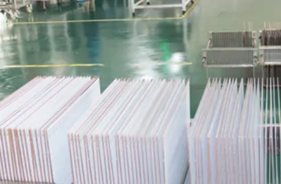
Step 1:Creating a designed layout on the copper-clad laminate
Step 2:PCB manufacturers will etch or remove excess material from inner layers to reveal images and pads.
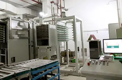
Step 3:Laminating printed circuit board materials at high temperatures for creating the PCB layer stack up
Step 4:Creating mounting holes, through-hole pins, and vias on PCB
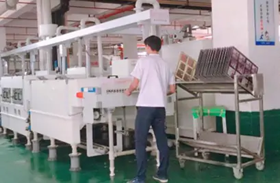
Step 5:Etching and removing the excess copper of the surface layer to reveal images and pads
Step 6:Placing plating pin holes and via holes
Step 7:Creating a protective coating or solder masking on the surface
Step 7:Silkscreen printing, logos or other markings, and installing polarity indicators on the surface
Есть вопросы? Обращайтесь к нам в любое время, и мы ответим на ваши запросы в течение 24 часов.
We specialize in building your pcb prototype and PCB assembly with rapid turn times.