
We use different electronic devices every day. For example, the computer or mobile phone you are using to read this article contains a complex PCB. Your television, kitchen stove, and even your digital watch also use PCBs. Have you ever wondered how factories produce thousands of PCBs every day? Have you ever thought about how the tiny copper traces on a PCB are made so precisely? That is where industrial PCB manufacturing comes in.
Industrial PCB manufacturing is highly precise. It makes thousands of PCBs look alike, even at the microscopic level. In this article, you will learn the steps followed in industry.
Processus de fabrication de PCB industriels
Industrial PCB manufacturing usually doesn’t involve small quantities. For large quantities, manual processes aren’t enough. As a result, factory owners invest more in automated production lines. They can make tens of thousands of PCBs every day. It is the only way they can meet tight shipping deadlines.
#1 PCB Design and BOM Preparation
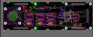
The first step in industrial PCB manufacturing is Conception de PCB. First, choose suitable PCB design software. In this case, you may consider Altium Designer, KiCad, Cadence, and EasyEDA.
In the software, you can decide where to place copper traces, electronic components, and drill holes. You can also choose how many layers your PCB needs. Once the design is complete, you can run simulations to check how the circuit should work.
After checking your design, export the Gerber and NC drill files. Finally, you send these files to the factory for production.
If you are a factory, you will need to prepare a Bill of Materials, or so-called BOM. It lists all the components needed to make your product.
#2 Circuit Pattern and Etching
After the design is ready, the next step in the industrial PCB manufacturing process is to create the circuit pattern.
Before creating the circuit pattern, the main board is already prepared. We won’t explain it in detail. However, note that the top layer of these boards is made of copper.
First, pass these boards into an automatic cleaning machine. It removes dirt and oxidation from the copper surface.
After cleaning, send these boards to the laminating area. Here, a laminating machine applies a dry film to the copper surface. It mainly contains the pre-printed circuit pattern.
Then, you will move the board to a special room with yellow lights. This is because the dry film is sensitive to blue light. The yellow light helps protect the film from unwanted exposure.
Next, you will expose the laminated board to UV light. It hardens the parts of the film that match the circuit pattern. The board then goes through another machine. This machine removes the soft, unexposed parts of the film. The remaining hard parts are called photoresist.
The photoresist protects the copper areas needed for the circuit pattern. Etching then removes the unwanted copper. This leaves only the required copper traces on the board.
After etching, the board goes through an Automated Optical Inspection (AOI) machine. The machine checks the circuit patterns for defects. An operator may also check the board manually. After AOI, the circuit pattern is ready.
#3 Layer Lamination & Drilling
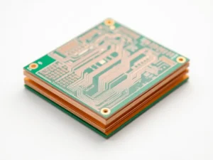
In the previous step, you created the circuit patterns of just one layer. However, a PCB may have more than that. It may need more circuit pattern layers, especially in HDI PCBs. In these situations, you repeat the previous process several times. Once all layers are ready, you join them and drill holes to connect them.
First, you stack the circuit layers with prepreg layers between them. Then, press them together in a vacuum lamination machine. It applies heat and pressure with high precision. As a result, the layers bond properly.
After lamination, an X-ray machine checks whether the layers are correctly aligned. It also helps us identify the exact drilling positions and creates the holes. A CNC machine usually does this job perfectly.

#4 Copper Plating and Circuit Formation
Now that the circuit patterns are properly organized and the holes are created, the circuit layers are still not connected. In this step of industrial PCB manufacturing, you will connect those holes using copper plating.
First, pass the PCB through a desmearing machine. It will clean the resin from the drilled holes. Once the holes are clean, add a thin layer of copper to their inner walls. Complete this process with electroless copper plating. Next, use electroplating to increase the copper thickness. The required thickness typically depends on the project’s needs. Finally, use an optical inspection machine to check whether you did this step correctly.
#5 Solder Mask and Surface Finishing
Now you have a complete PCB in your hand. But there’s still a problem: your circuits are exposed and at risk of short circuits. So, you need to cover them. Therefore, the next step is solder mask and surface finishing. It is one of the crucial steps in the industrial pcb manufacturing process.
First, apply the solder mask to the board using an automatic screen-printing or spray-coating machine. Later, pass the board into a drying oven at around 87°C. This helps the solder mask harden and prepare for the next step.
Now the board has the solder mask. But you still need to expose the solder pad, right? So, you will need to apply another film just for those solder pads. Then you pass it through a UV exposure machine again. This process removes the solder mask from those specific areas.
After that, the board goes through a steel screen-printing machine. This machine adds labels and markings to the PCB. These markings help identify components and their positions. For example, R represents a resistor, and C represents a capacitor. Plus (+) and minus (−) signs indicate positive and negative terminals. GND marks the ground connection.

#6 PCB Cutting, Inspection and Testing
The final step in the industrial PCB manufacturing process is preparing the PCB for shipping.
During manufacturing, manufacturers often make several PCBs on a single large board. The number may range from two to fifty or more. The exact number typically depends on the PCB’s size. Before shipping, they must separate and pack these boards individually for protection.
First, verify each PCB’s quality. Several verification methods are available. You can use a flying probe testing machine to check the circuit connections. You can also use an AOI machine to check whether the labels and markings are correct.
Next, separate the individual PCBs from the large board. You can do this using a CNC routing machine or a V-cut machine.
After cutting, inspection, and testing, the PCBs are ready for the next stage. You can send them for assembly or ship them to your customer’s factory for Assemblée.
Réflexions finales
In this article, we have explored an overview of the industrial PCB manufacturing process. We have not covered every detail. However, we have tried to cover how printed circuit boards are made in industrial settings.
Precision is the most important factor in PCB fabrication. Maintaining the same quality across all printed circuit boards is tricky. That is why machine selection and proper quality control matter. UETPCB is equipped with many advanced machines. Our skilled operators have years of industry experience.
If you have any questions about PCBs, contactez our customer support team. We are always ready to help. Our company provides a wide range of electronics manufacturing services, from PCB fabrication to Assemblage de PCB.