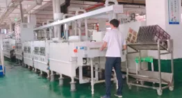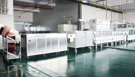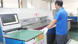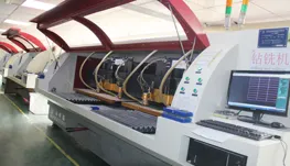
Pcb prototype service introduction
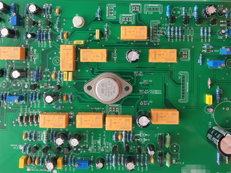
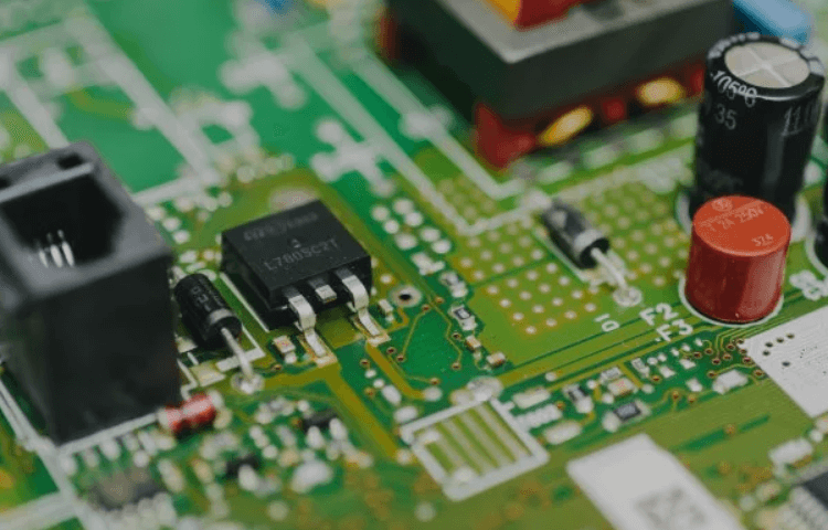
Component assembly
| Feature | Through-Hole | SMT (Tecnologia de Montagem em Superfície) |
|---|---|---|
| Component Type | Long-leaded, larger components (e.g., electrolytic capacitors, transformers) | Compact, leadless components (e.g., SMD resistors, ICs) |
| Projeto de placas de circuito impresso | Requires drilled holes (common for single/double-layer boards) | No drilling needed (ideal for high-density multilayer boards) |
| Mechanical Strength | High (suitable for physical stress or high-temperature environments) | Lower (relies on solder paste adhesion) |
| Cost/Efficiency | Higher labor costs (ideal for prototypes/low-volume) | Highly automated (optimized for mass production) |
Manual and automated Insertion
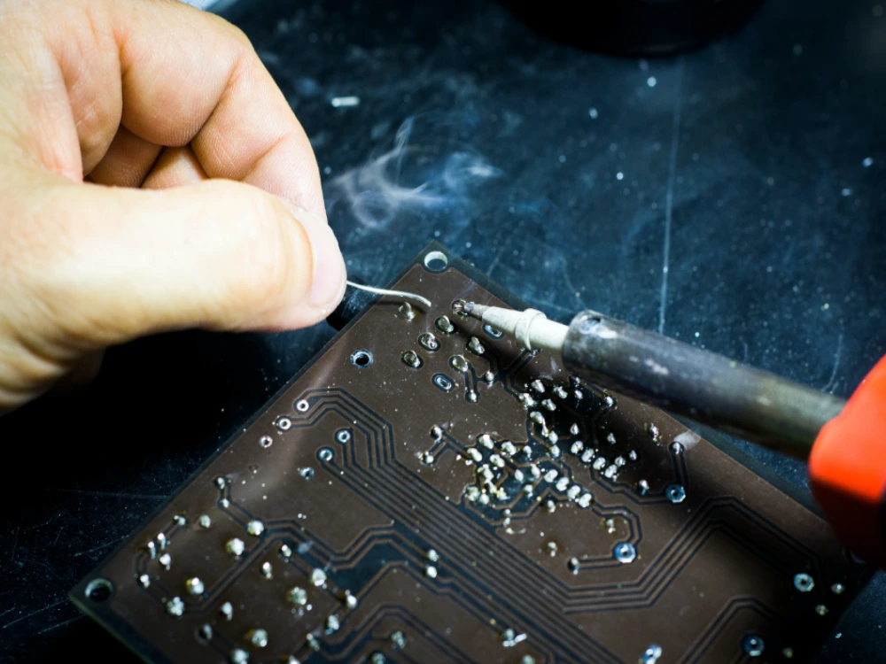
Lead-free or RoHS soldering
Double Wave Flow Solder
Selective wave soldering
Use low and high melting point solder
Conformal Coating
IC Programming
Inspection and functional testing
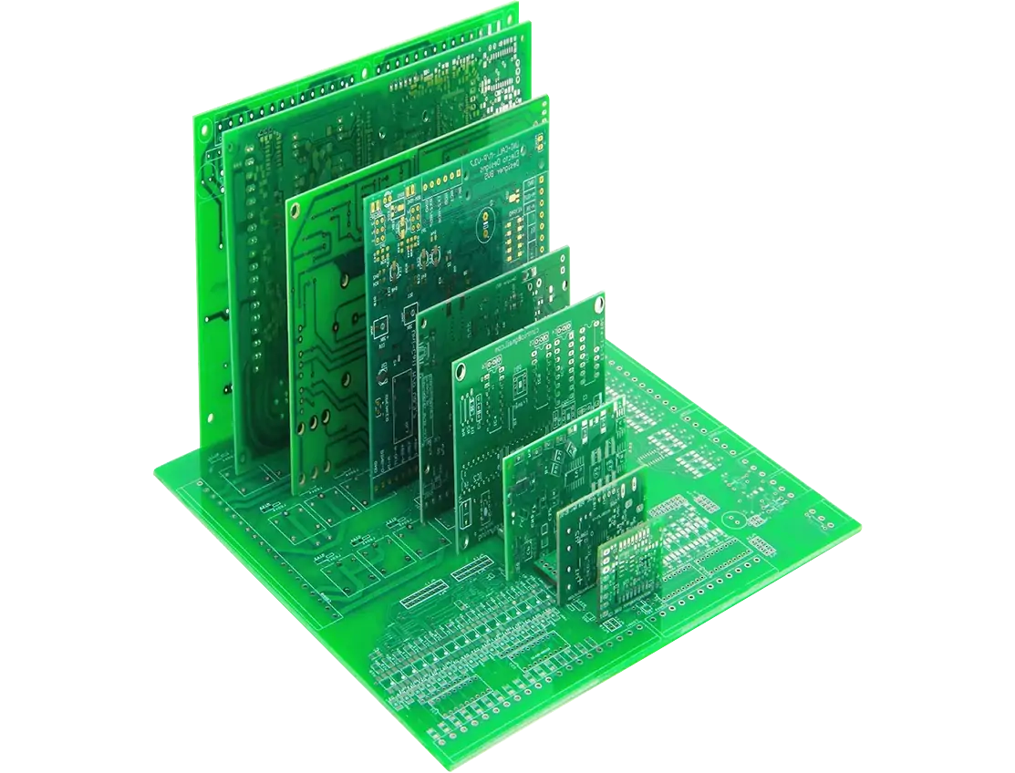
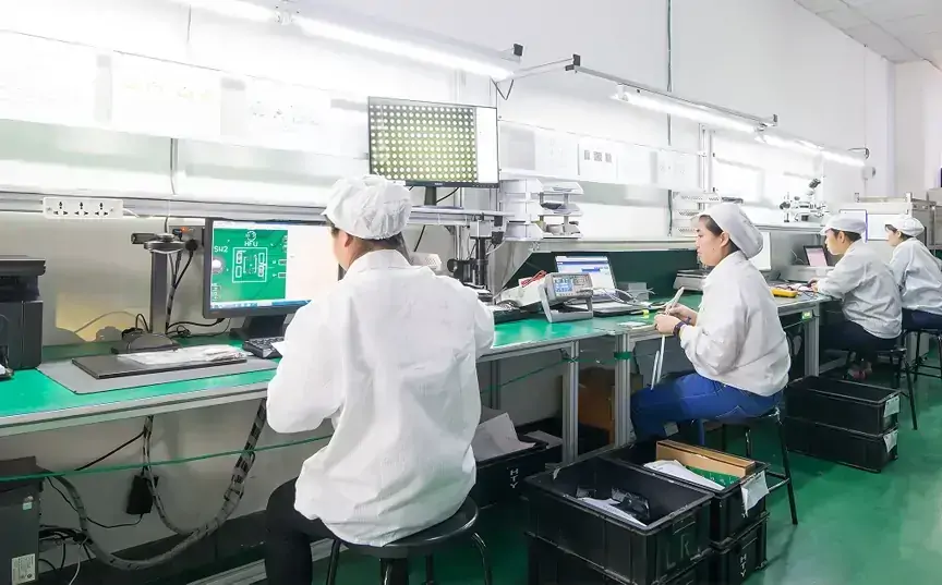
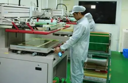
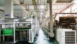
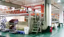
A UETPCB é uma fornecedora profissional de placas de circuito impresso (PCB) e fabricante de montagem de placas de circuito impresso (PCBA) em Shenzhen. Nosso foco é oferecer serviços de montagem de PCB de alta qualidade. Como fornecedora confiável de PCB, oferecemos um serviço completo, desde a fabricação até a montagem das placas. Nossa equipe profissional possui a experiência e as habilidades necessárias para atender às necessidades de diversos setores. Nosso objetivo é ser seu parceiro preferencial na fabricação de PCBA na China. Se você precisar de serviços de montagem de PCB de qualidade, entre em contato conosco.
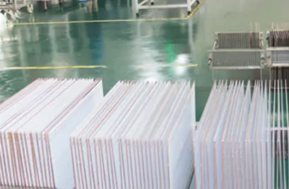
Step 1:Creating a designed layout on the copper-clad laminate
Step 2:PCB manufacturers will etch or remove excess material from inner layers to reveal images and pads.
Step 3:Laminating printed circuit board materials at high temperatures for creating the PCB layer stack up
Step 4:Creating mounting holes, through-hole pins, and vias on PCB
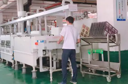
Step 5:Etching and removing the excess copper of the surface layer to reveal images and pads
Step 6:Placing plating pin holes and via holes
Step 7:Creating a protective coating or solder masking on the surface
Step 7:Silkscreen printing, logos or other markings, and installing polarity indicators on the surface
Alguma dúvida? Entre em contato conosco a qualquer momento, e responderemos às suas perguntas em até 24 horas.
We specialize in building your pcb prototype and PCB assembly with rapid turn times.