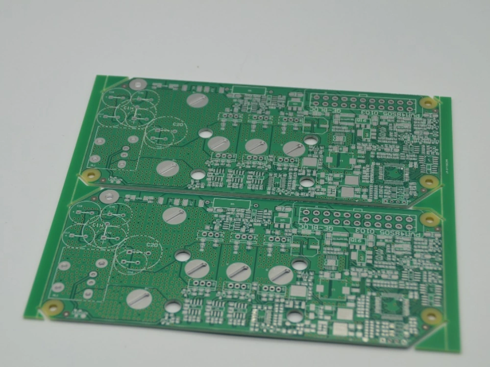
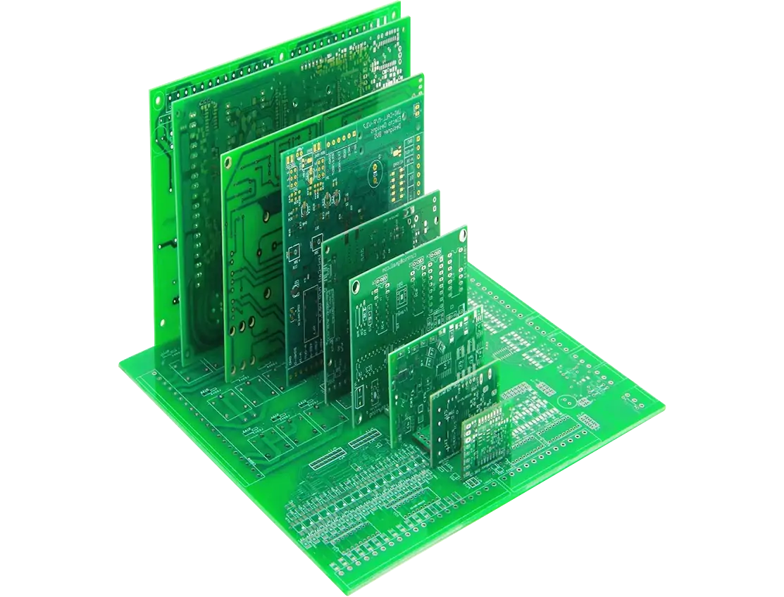
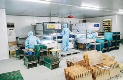
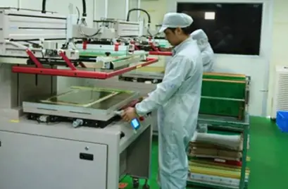
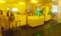
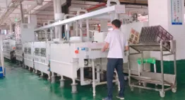
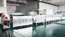
Pcb prototype service introduction
Component assembly
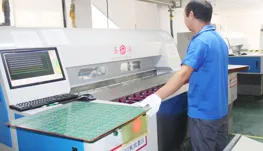
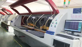
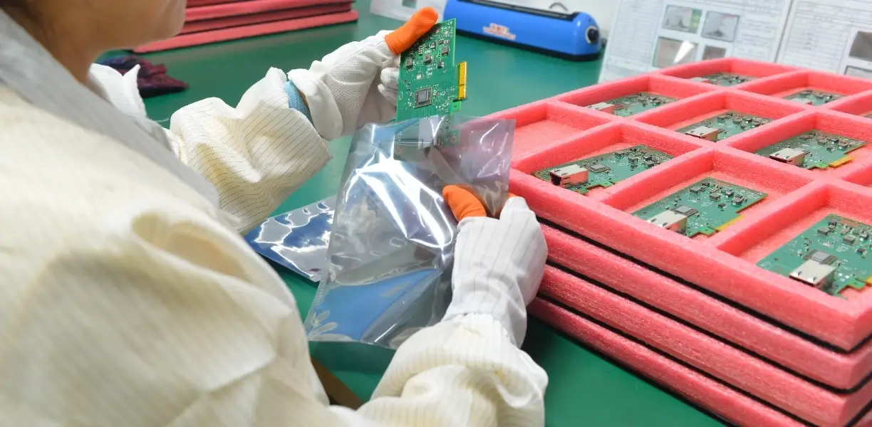
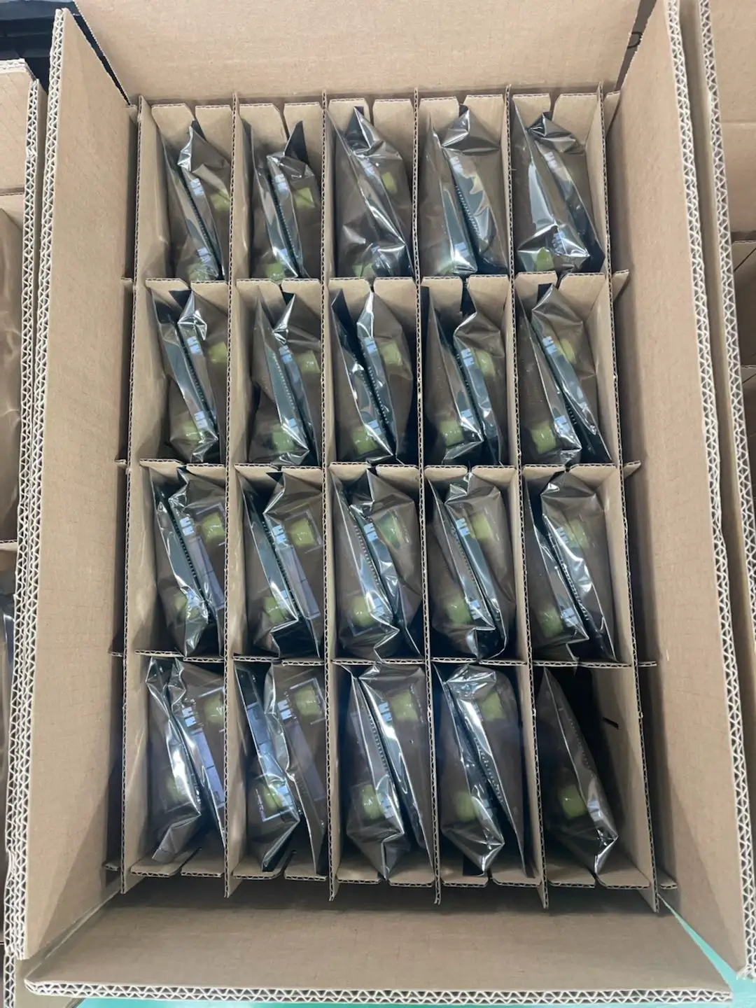
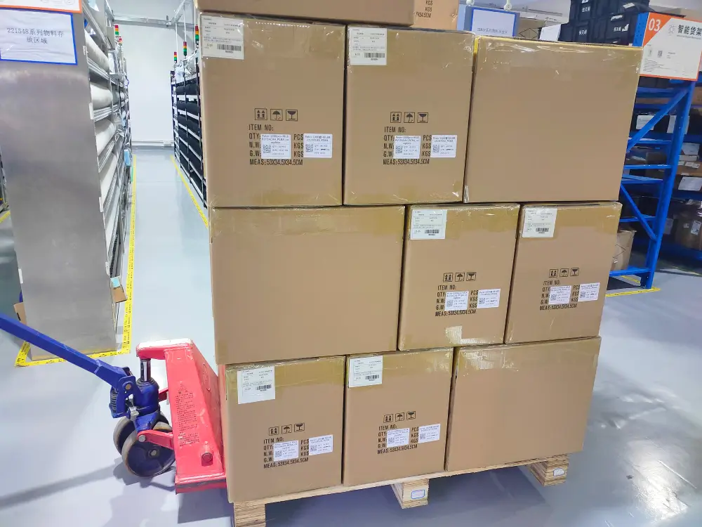
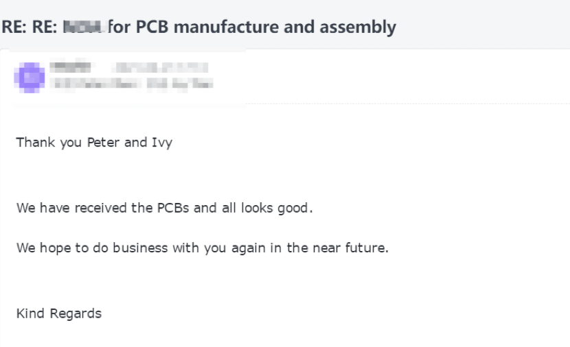
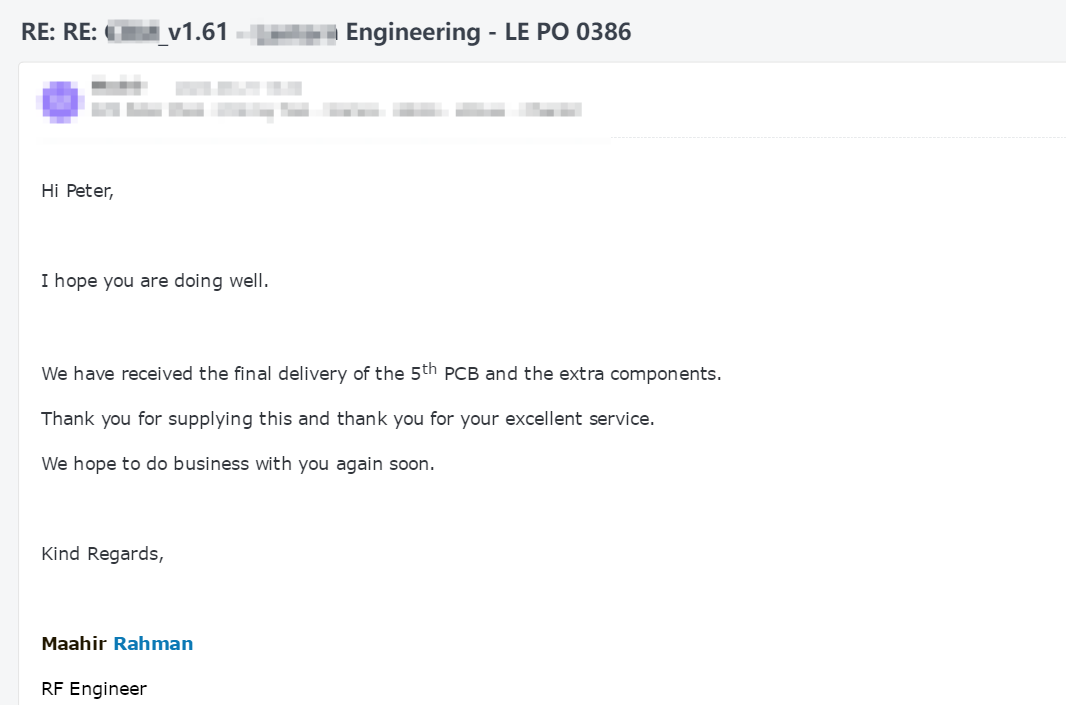
UETPCB è un fornitore professionale di circuiti stampati e produttore di assemblaggi PCB con sede a Shenzhen. Ci specializziamo nella fornitura di servizi di assemblaggio PCB di alta qualità. In qualità di fornitore affidabile di circuiti stampati, offriamo un servizio completo, dalla produzione dei circuiti stampati all’assemblaggio. Il nostro team di professionisti vanta l’esperienza e le competenze necessarie per soddisfare le esigenze di diversi settori industriali. Il nostro obiettivo è diventare il vostro partner di riferimento nella produzione di circuiti stampati assemblati (PCBA) in Cina. Se avete bisogno di servizi di assemblaggio di circuiti stampati di qualità, non esitate a contattarci.
| Features | Available |
|---|---|
| Sizes | Maximum 610*1100mm / Minimum 5*6mm |
| Quantity | 1-1million pcs |
| layers | 1-48 layers |
| Min. Line Width | 0.076mm/3mil |
| Min. drilled hole size | 0.08mm [0.003″] |
| Min. line spacing | 0.075mm (3mil) |
| Copper Thickness | 1oz—13oz 0.25oz-10.0oz |
| Base Material | Aluminum, FR4, Flex, Flex-rigid, HDI, Rogers, etc. |
| Board Thickness | ≥0.1mm |
| Surface Finish/Treatment | HALS/HALS lead free, Immersion gold, OSP, Hard Gold, ENEIG, Immersion sliver, etc |
| Finish Cooper | 1-13oz |
| Solder Mask Color | Green, Red, Yellow, Blue, White, Black, Purple, Matte Black, Matte green |
| Silkscreen | White, Black |
| Testing | Fly Probe Testing (Free) and A.O.I. testing |
| Build time | 24 hours |
| Lead time | 2-3 days |
Step 1:Creating a designed layout on the copper-clad laminate
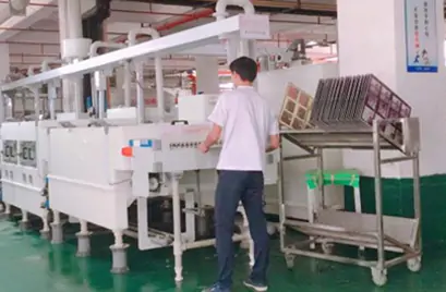
Step 2:PCB manufacturers will etch or remove excess material from inner layers to reveal images and pads.
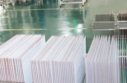
Step 3:Laminating printed circuit board materials at high temperatures for creating the PCB layer stack up
Step 4:Creating mounting holes, through-hole pins, and vias on PCB
Step 5:Etching and removing the excess copper of the surface layer to reveal images and pads
Step 6:Placing plating pin holes and via holes
Step 7:Creating a protective coating or solder masking on the surface
Step 7:Silkscreen printing, logos or other markings, and installing polarity indicators on the surface
Hai domande? Contattaci in qualsiasi momento: risponderemo alle tue richieste entro 24 ore.
We specialize in building your pcb prototype and PCB assembly with rapid turn times.