Assemblaggio di circuiti stampati con fori passanti

pcb wholesale

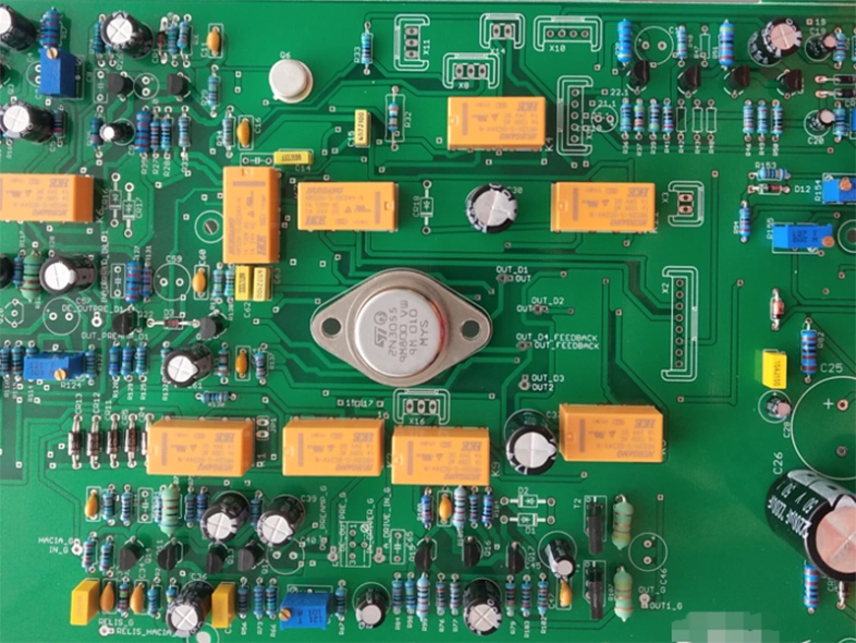
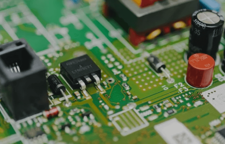
Through-Hole PCB Assembly is a traditional electronic component assembly method. It is mainly used to mount components with long pins on PCB. Its core feature is that the pins of the components pass through the pre-drilled holes on the PCB and are fixed on the other side of the board by welding.

Pcb prototype service introduction

Component assembly

It’s crucial to work with a reliable PCB prototype manufacturer. We can fabricate the sample boards quickly. If you need some printed circuit boards, contact us now. UETPCB offers quick-turn PCB prototype services for PCB manufacturing and assembly at high quality and low cost.

Produttore cinese di assemblaggi di circuiti stampati – UET PCB

UETPCB è un fornitore professionale di circuiti stampati e produttore di assemblaggi PCB con sede a Shenzhen. Ci specializziamo nella fornitura di servizi di assemblaggio PCB di alta qualità. In qualità di fornitore affidabile di circuiti stampati, offriamo un servizio completo, dalla produzione dei circuiti stampati all’assemblaggio. Il nostro team di professionisti vanta l’esperienza e le competenze necessarie per soddisfare le esigenze di diversi settori industriali. Il nostro obiettivo è diventare il vostro partner di riferimento nella produzione di circuiti stampati assemblati (PCBA) in Cina. Se avete bisogno di servizi di assemblaggio di circuiti stampati di qualità, non esitate a contattarci.

single_sided_Easy_to_Repair

Through-Hole  Vs SMT

Feature Through-Hole SMT (Surface Mount Technology)
Component Type Long-leaded, larger components (e.g., electrolytic capacitors, transformers) Compact, leadless components (e.g., SMD resistors, ICs)
Progettazione di circuiti stampati Requires drilled holes (common for single/double-layer boards) No drilling needed (ideal for high-density multilayer boards)
Mechanical Strength High (suitable for physical stress or high-temperature environments) Lower (relies on solder paste adhesion)
Cost/Efficiency Higher labor costs (ideal for prototypes/low-volume) Highly automated (optimized for mass production)

Steps for Through-Hole PCB Assembly

  1. Drilling
    Hole matching the pins of components is pre-drilled on the PCB, usually with a larger diameter (such as more than 1mm).
  2. Component Insertion
    The pins of the components pass through the holes, usually done manually or by an automatic insertion machine.
  3. Soldering
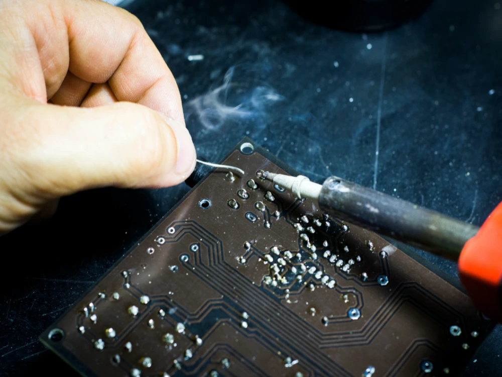
    The pins are fixed to the PCB pads by wave soldering or manual soldering to form an electrical connection.
Security_Industry_PCB
IQC_Incoming_Material_Inspection

Our Through-hole Assembly Capabilities

Manual and automated Insertion
Lead-free or RoHS soldering
Double Wave Flow Solder
Selective wave soldering
Use low and high melting point solder
Conformal Coating
IC Programming
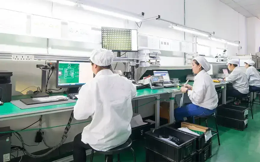
Inspection and functional testing

Produttore cinese di assemblaggi di circuiti stampati

UETPCB è un fornitore professionale di circuiti stampati e produttore di assemblaggi PCB con sede a Shenzhen. Ci specializziamo nella fornitura di servizi di assemblaggio PCB di alta qualità. In qualità di fornitore affidabile di circuiti stampati, offriamo un servizio completo, dalla produzione dei circuiti stampati all’assemblaggio. Il nostro team di professionisti vanta l’esperienza e le competenze necessarie per soddisfare le esigenze di diversi settori industriali. Il nostro obiettivo è diventare il vostro partner di riferimento nella produzione di circuiti stampati assemblati (PCBA) in Cina. Se avete bisogno di servizi di assemblaggio di circuiti stampati di qualità, non esitate a contattarci.
Richiedi subito un preventivo

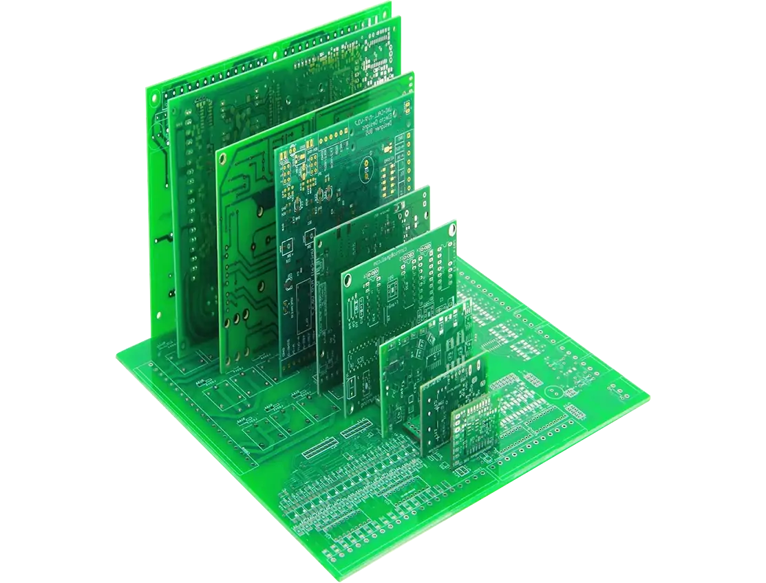
PCB Fabrication Process

Step 1:Creating a designed layout on the copper-clad laminate

Step 2:PCB manufacturers will etch or remove excess material from inner layers to reveal images and pads.
Step 3:Laminating printed circuit board materials at high temperatures for creating the PCB layer stack up

Step 4:Creating mounting holes, through-hole pins, and vias on PCB

Step 5:Etching and removing the excess copper of the surface layer to reveal images and pads

Step 6:Placing plating pin holes and via holes

Step 7:Creating a protective coating or solder masking on the surface

Step 7:Silkscreen printing, logos or other markings, and installing polarity indicators on the surface

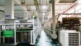
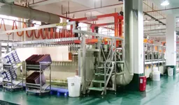
PCB Production Equipment

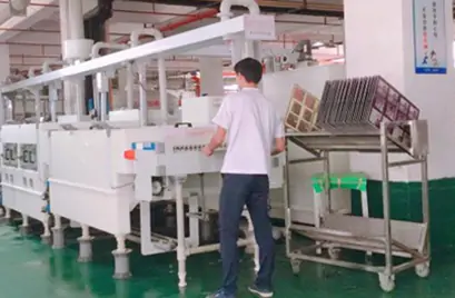
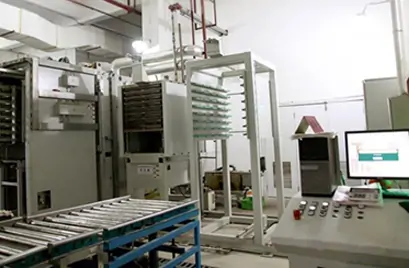
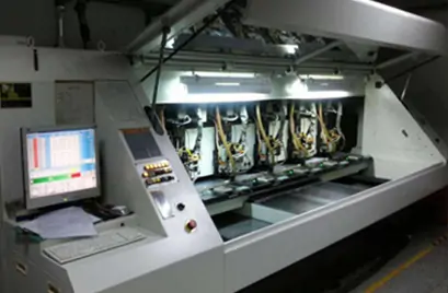
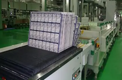
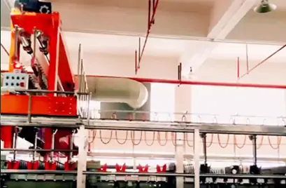
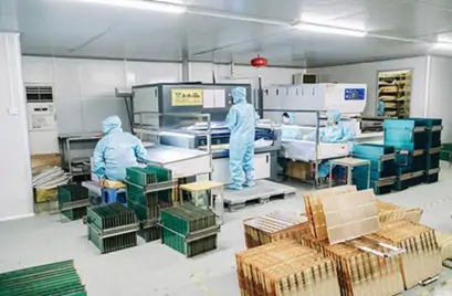
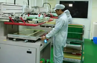
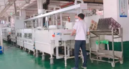
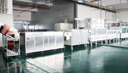
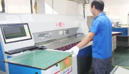
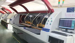
UETPCB uses advanced production machinery to ensure precise, efficient. These amazing machines create flawless boards, and save time. Here are our some  equipment.

Our Certifications

Our electronic contract manufacturing and PCB manufacturing service has developed trust among customers. This trust is a result of our unwavering commitment to quality. Whether a small volume or a large production run, the boards we fabricate always comply with the following standards.

  • ISO 9001
  • ISO 13485
  • UL
  • RoHS
  • IATF16949
  • IPC-A-610E

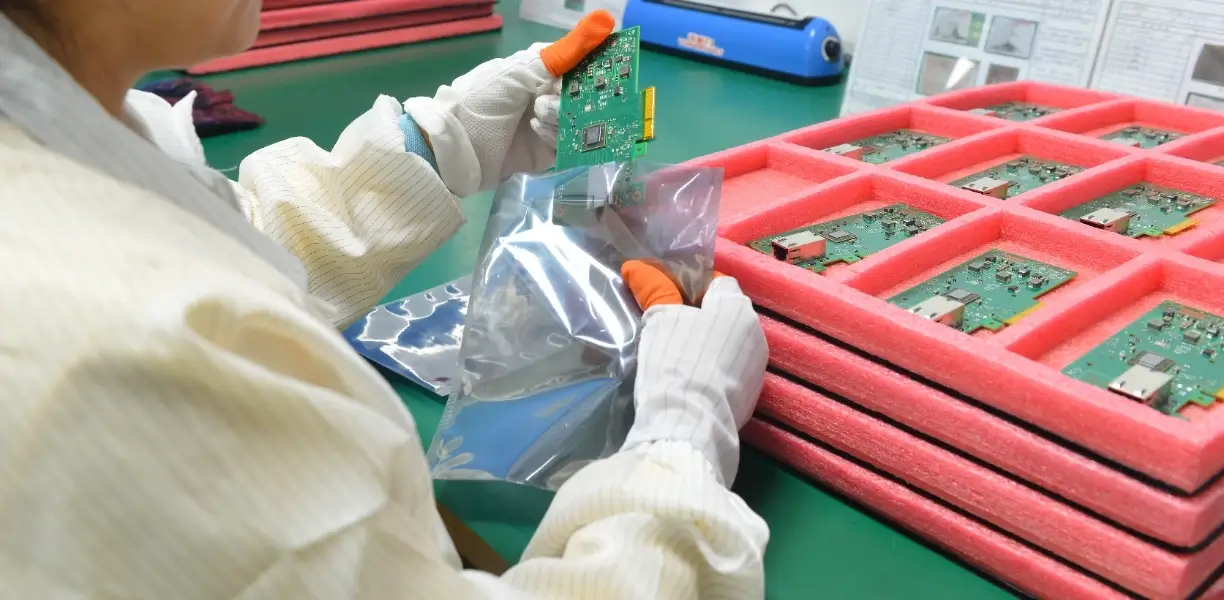
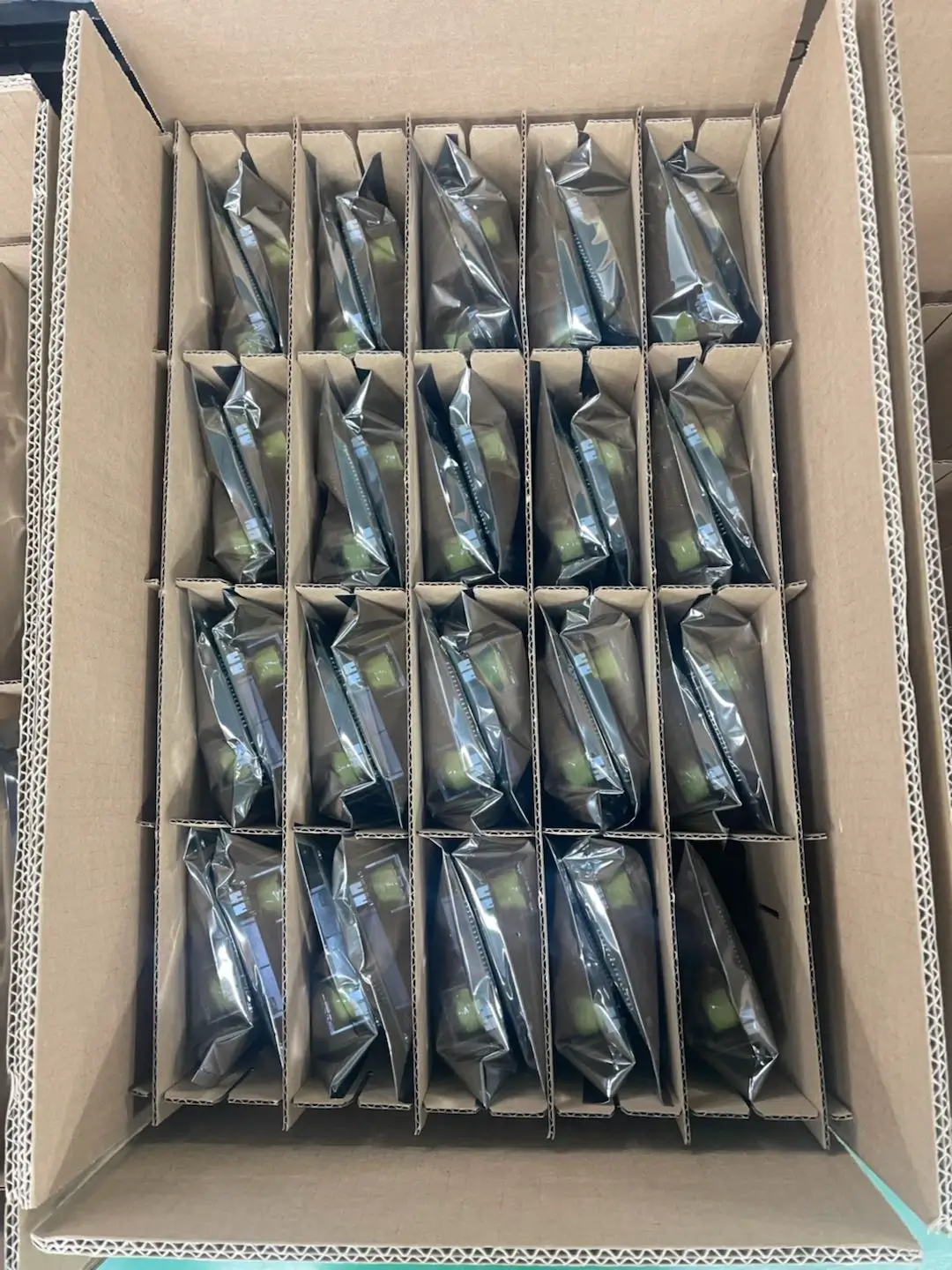
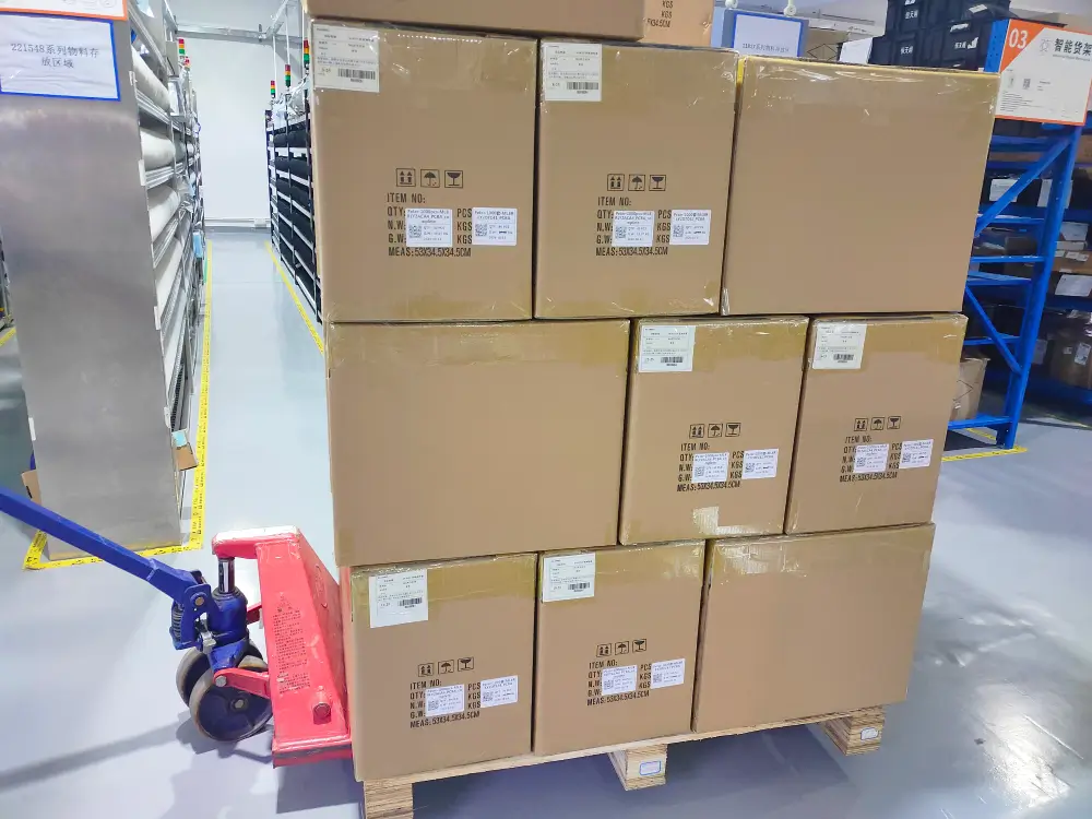
I nostri imballaggi

PCB_involucro
Confezionamento dei circuiti stampati
Imballaggio delle schede elettroniche

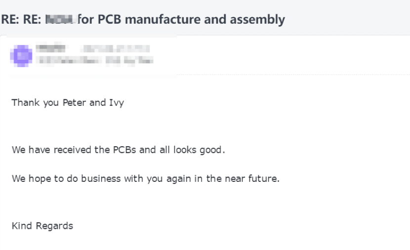
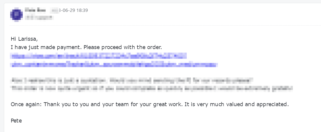
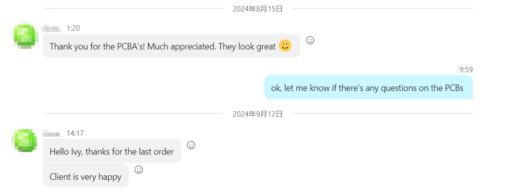
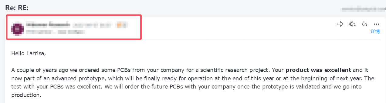
Cosa dicono i nostri clienti dei nostri servizi PCBA

Siamo qui per aiutarti

Hai domande? Contattaci in qualsiasi momento: risponderemo alle tue richieste entro 24 ore.

We specialize in building your pcb prototype and PCB assembly with rapid turn times.


    Please prove you are human by selecting the key.