HDI PCB定義
HDI 板被定義為與標準 PCB 相比,將更多電路封裝到較小的區域中的印刷電路板。 HDI板有以下幾種類型:
- 1.I型
- 2.II型
- 3.Ⅲ型
每種類型都具有 IPC-2226 標準中概述的不同功能。
如果您需要更多資訊或協助,請聯絡我們。我們隨時為您提供協助!
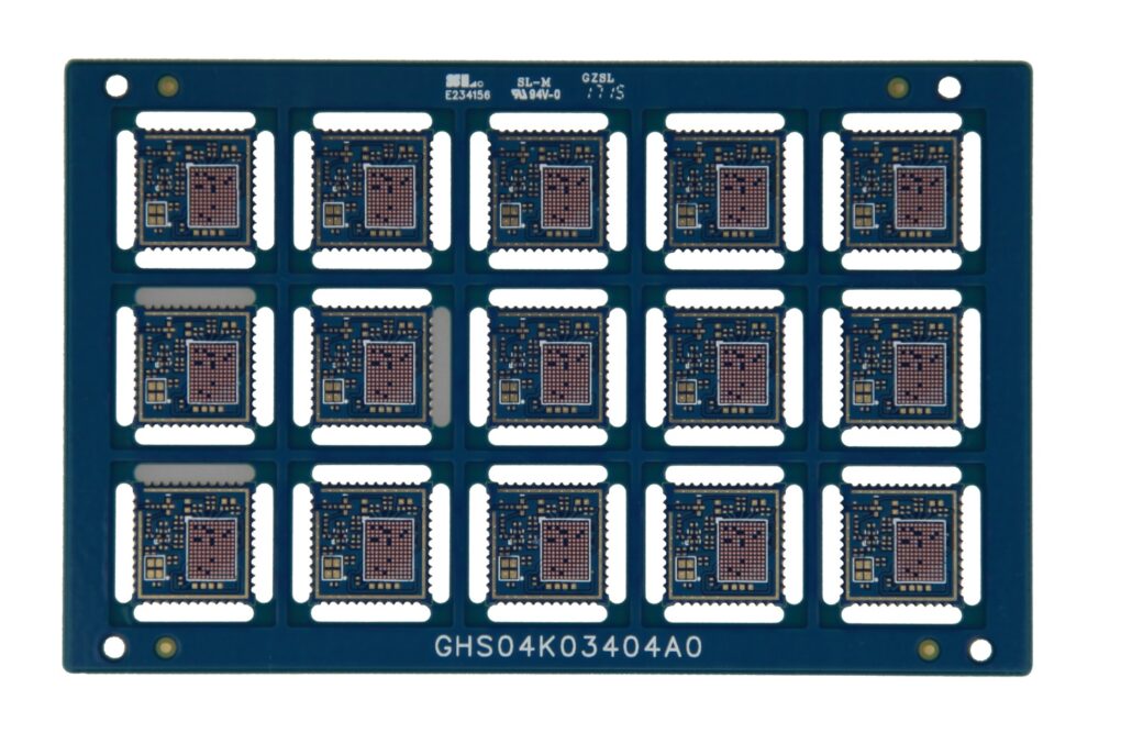
我們的 HDI PCB 能力
| 獨特之處 | 規範 |
|---|---|
| 層數 | 4 – 22層標準,30層高級 |
| 專業技術 | 多層 PCB 的連接焊盤比標準板更密集。它們包括更精細的線條和空間。該板還具有較小的孔和捕獲墊。這種設計允許微通孔穿透選定的層並整合到表面焊盤中 |
| HDI 構建 | 1+N+1、2+N+2、3+N+3,4+N+4、任意層/ELIC、Ultra HDI研發 |
| 材料 | FR4 標準、FR4 高性能、無鹵 FR4、羅傑斯 |
| 銅配重(成品) | 18μm – 70μm |
| 最小軌道和間隙 | 0.075mm / 0.075mm |
| PCB厚度 | 0.40毫米– 10.0毫米 |
| 最大尺寸 | 800毫米×950毫米;取決於雷射鑽孔機 |
| 可用表面處理 | OSP、ENIG、沉錫、沈銀、電解金、金手指 |
| 最小機械鑽 | 0.15mm |
| 最小雷射鑽孔 | 標準0.10mm,高級0.075mm |
HDI PCB Design
The process of HDI PCB design consists of these main steps:

需求分析
The performance requirements must 被拼寫出來 first. These include the size constraints and board cost targets.
原理圖設計
Design the circuit connections; figure out how components are linked.

PCB佈局
Translate circuit schematics into specific PCB design drawings. At this stage, we need to place components and optimize routing for electrical performance to minimize signal interference.
Via Hole (Vias) Configuration
Via hole technology is critical in HDI PCB design, so decide on via hole sizes and locations to support multi-layer connections.

模擬測試
Electronic simulation tests a design before it 已製造 and checks whether or not it is valid and performs as expected within a system.

原型製造
Make PCB prototypes based on design drawings – this part verifies theory through practice.

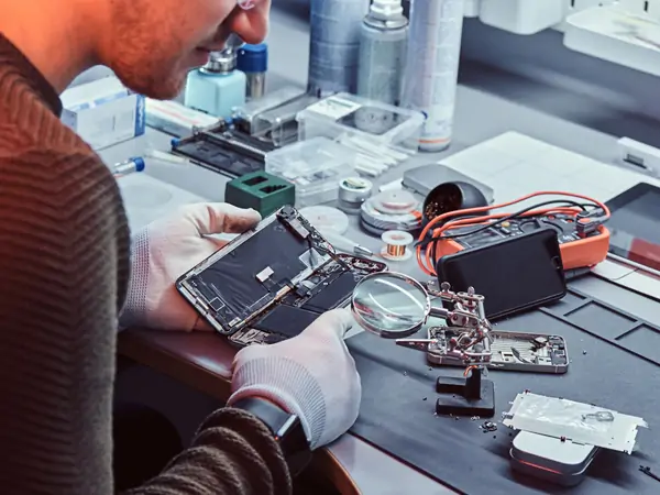
Testing & Debugging
Test the prototype board’s functionality and speed, adjusting where necessary to fix design errors.

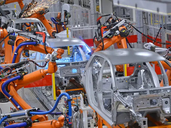
大量生產
Start mass production once the prototype has been checked and found correct.


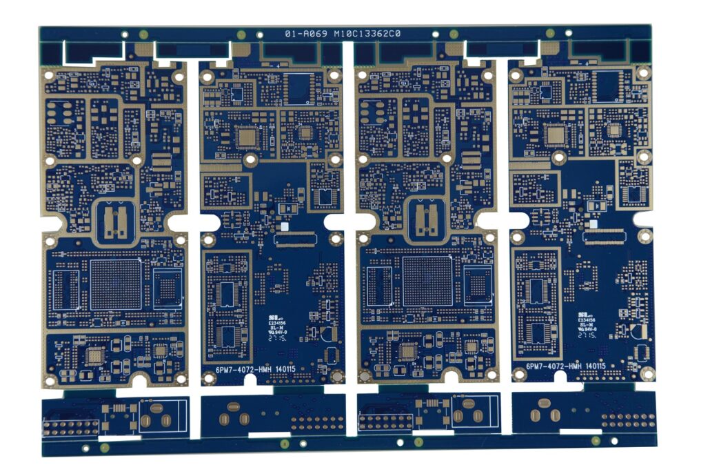
Our HDI PCB Technology
HDI technology is a high-end technology used to manufacture HDI PCBs. This printed circuit board features high density and exemplary performance in circuit interconnection.
根據過孔的不同,HDI板可分為六種不同類型:
- ⚫ Face-to-face through vias
- ⚫ Through vias and buried vias
- ⚫ Two or more layers with through vias
- ⚫ Non-electrical connection and passive substrate
- ⚫ Coreless construction with layer pairs
- ⚫ Alternate constructions of coreless constructions with layer pairs
- ⚫ HDI Printed Circuit Board Manufacturing
Advanced HDI Technology Methods
- Via in-pad process:
In this process, HDI PCB manufacturers place bias on the surface of the flat lands. Then, they fill the vias with conductive or non-conductive epoxy. Later, they are capped and plated over, making the via invisible. - 過孔填充技術:
Specific materials include silver-filled, conductive epoxy, non-conductive epoxy, electrochemical plating, and copper-filled. - 非常規HDI PCB構建:
HDI PCBs must combine more lines and annular rings on a thin, high-density board. - 激光鑽孔技術:
A laser beam 20 microns in diameter can create the smallest vias on the surface of HDI PCBs. This high-energy light is precise and efficient and can cut through metal and glass to make a tiny hole.
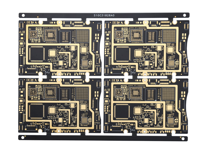
HDI PCB Application & Advantages
雖然 HDI PCB has a complex manufacturing process, it has a wide range of applications. It can be used in various industries, such as electronics and medical. The lighter weight and small size give it appropriate reasons to be installed in miniature equipment.
HDI PCB 是由消費者驅動的,適合更精緻和複雜的電子設備。 如今,人們更喜歡敏捷電子設備,因為它方便、輕巧。 HDI PCB使設備小型化、智慧化。 它輕薄,具有高端技術和高速運算能力。


Your Reliable HDI PCB Manufacturing
High-density interconnection technology
Our HDI PCB uses high-density interconnections, which allow it to support many more electrical connections in a limited area.
高品質材料和製造工藝
We use the best materials and most advanced techniques. We also ensure that HDI PCBs perform at a top level of electrical performance.

定制服務
Here, we offer you custom solutions for HDI PCB. We tailor-make our designs and manufacturing to fit what you want them to be like.

Fast delivery and quality service
We have streamlined production processes. What’s more, we work with professional teams that guarantee you get the best quality HDI PCBs.
立刻與我們聯繫
Have any needs or quotation inquiries about HDI PCB? Don’t hesitate, fill out the form below and we will contact you as soon as possible!