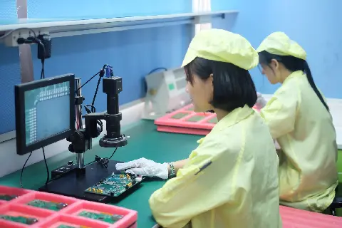
SMT PCB Assembly Supplier

quality_control PCB manufacturers

Are you seeking a trustworthy SMT PCB assembly supplier? UETPCB provides high-quality surface mount technology services. We guarantee fast delivery of your orders – full-process service from prototype design to bulk order. Contact us now to get PCB solutions!

Pcb prototype service introduction

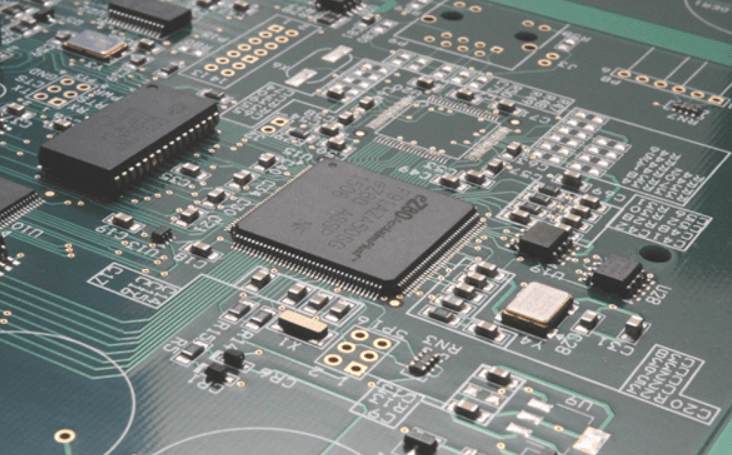
Component assembly

It’s crucial to work with a reliable PCB prototype manufacturer. We can fabricate the sample boards quickly. If you need some printed circuit boards, contact us now. UETPCB offers quick-turn PCB prototype services for PCB manufacturing and assembly at high quality and low cost.
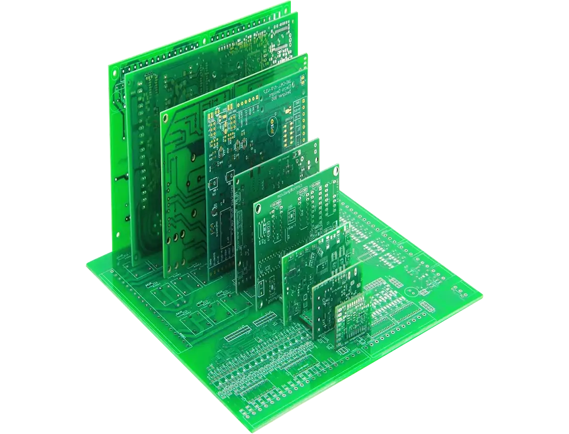
中国PCB组装制造商——UET PCB

UETPCB 是位于深圳的专业 PCB 供应商及 PCBA 制造商。我们专注于提供高质量的 PCB 组装服务。作为一家值得信赖的 PCB 供应商,我们提供从 PCB 制造到组装的一站式服务。我们的专业团队拥有丰富的经验和专业技能,能够满足各行各业的需求。 我们的目标是成为您在中国PCBA制造领域的首选合作伙伴。如果您需要优质的PCB组装服务,请联系我们。

中国PCB组装制造商

UETPCB 是位于深圳的专业 PCB 供应商及 PCBA 制造商。我们专注于提供高质量的 PCB 组装服务。作为一家值得信赖的 PCB 供应商,我们提供从 PCB 制造到组装的一站式服务。我们的专业团队拥有丰富的经验和专业技能,能够满足各行各业的需求。 我们的目标是成为您在中国PCBA制造领域的首选合作伙伴。如果您需要优质的PCB组装服务,请联系我们。

立即获取报价

PCBA-SMT组装

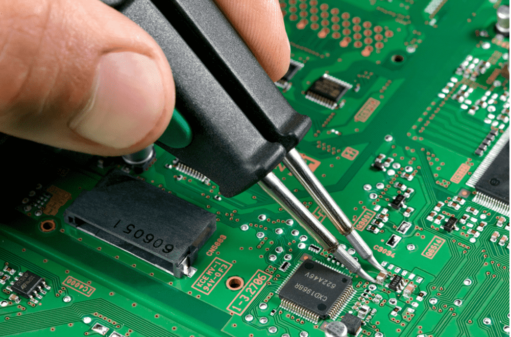
PCB SMT Assembly Process

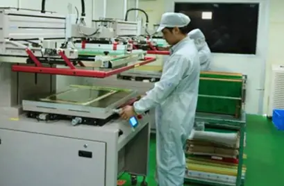
  1. Solder paste printing: Precisely apply solder paste on PCB pads;
  2. Component placement: Place SMD components on pads by high-speed placement machines;
  3. Reflow soldering: High-temperature heating melts the solder paste and forms a reliable connection;
  4. Inspection and testing: Use AOI (Automatic Optical Inspection) and X-ray to ensure quality.

Advantages of SMT PCB assembly

✅ High-density design: supports smaller and lighter electronic devices (such as mobile phones, smart hardware);
✅ Automated production: fast speed, high precision, suitable for mass production;
✅ Cost-effectiveness: reduces labor and material waste, lowers unit cost;
✅ High-frequency performance: shortens signal path and improves high-speed circuit stability.

pcb assembly process SMT

PCB Fabrication Process

Step 1:Creating a designed layout on the copper-clad laminate

Step 2:PCB manufacturers will etch or remove excess material from inner layers to reveal images and pads.

Step 3:Laminating printed circuit board materials at high temperatures for creating the PCB layer stack up

Step 4:Creating mounting holes, through-hole pins, and vias on PCB

Step 5:Etching and removing the excess copper of the surface layer to reveal images and pads

Step 6:Placing plating pin holes and via holes

Step 7:Creating a protective coating or solder masking on the surface

Step 7:Silkscreen printing, logos or other markings, and installing polarity indicators on the surface

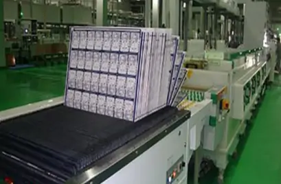
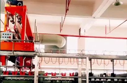
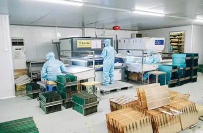
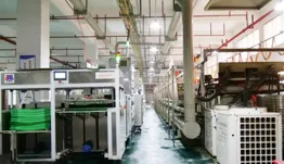
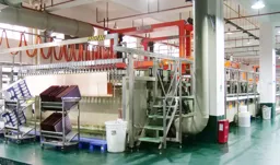
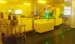
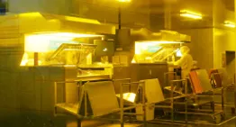
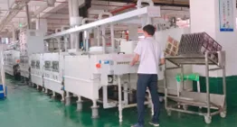
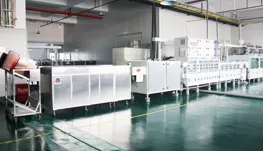
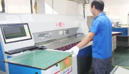
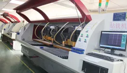
PCB Production Equipment

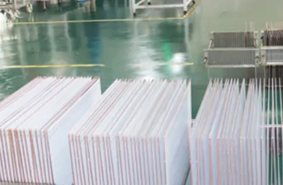
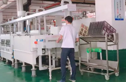
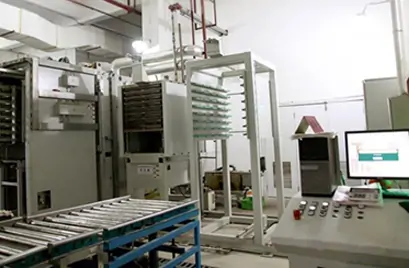
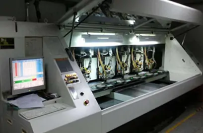
UETPCB uses advanced production machinery to ensure precise, efficient. These amazing machines create flawless boards, and save time. Here are our some  equipment.
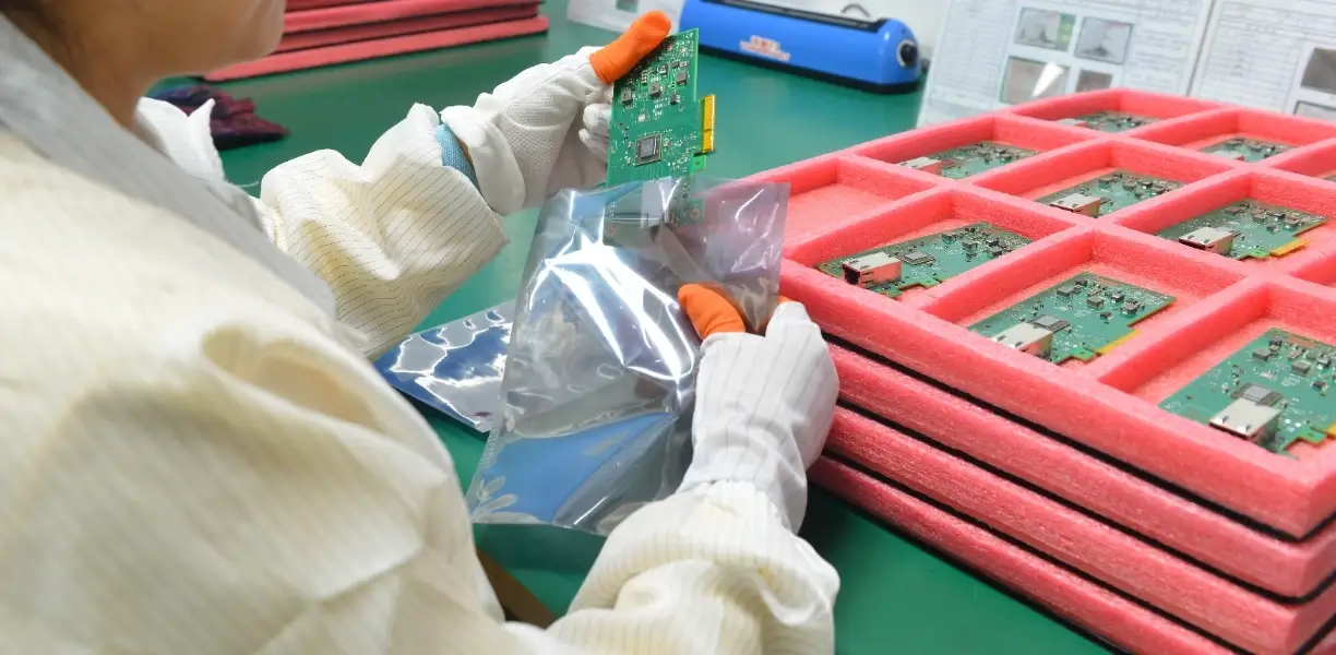
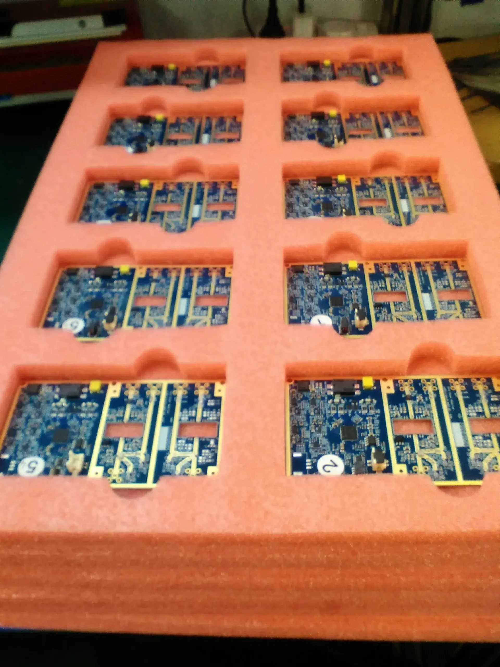
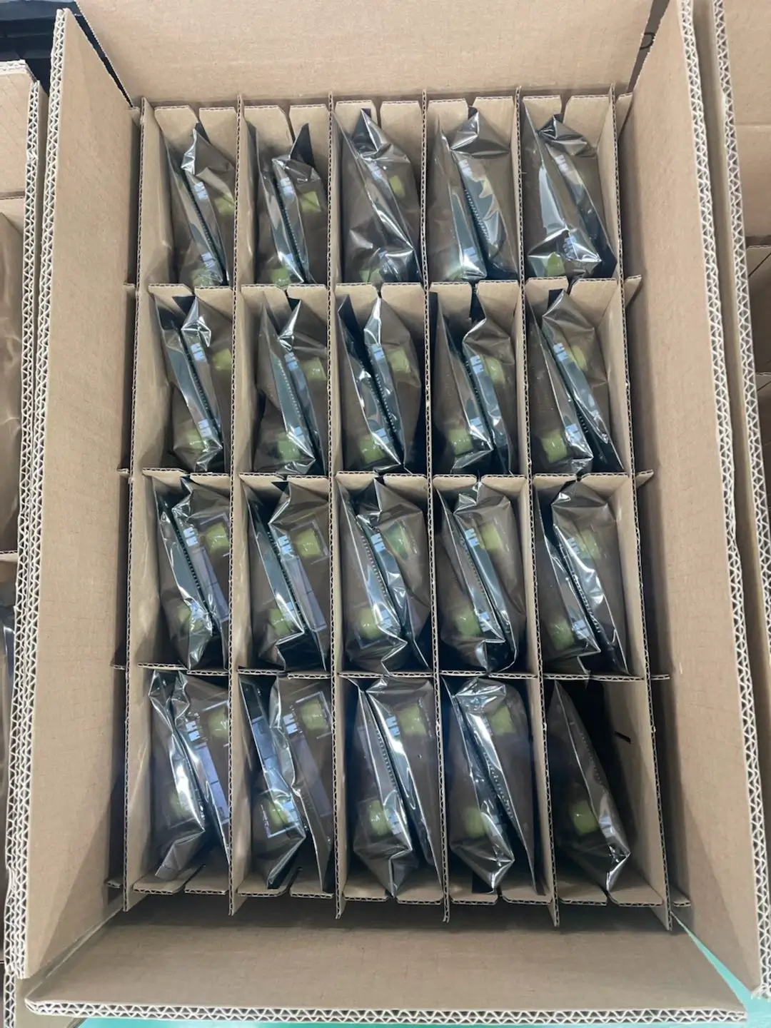
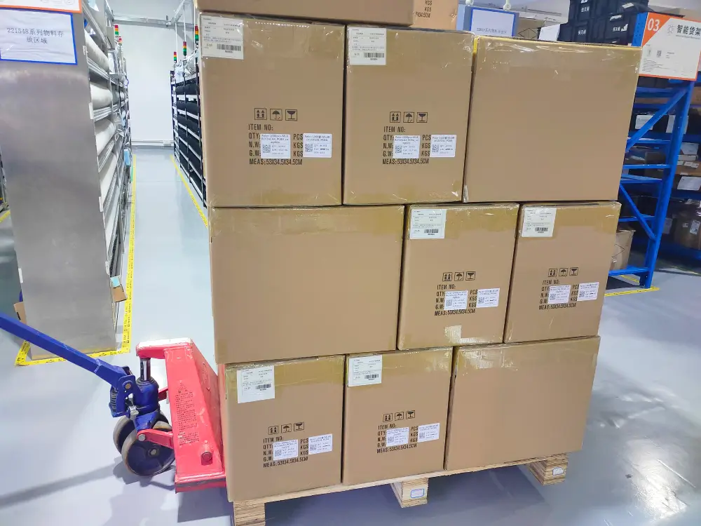
我们的包装

PCB_外壳
电路板封装
印刷电路板封装
电子电路板封装

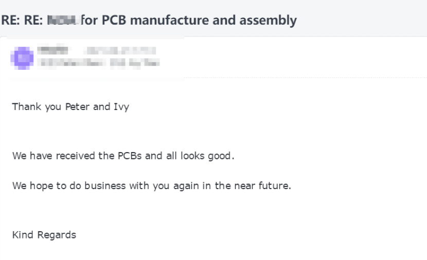
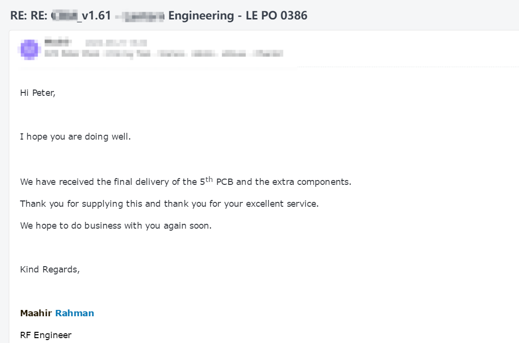
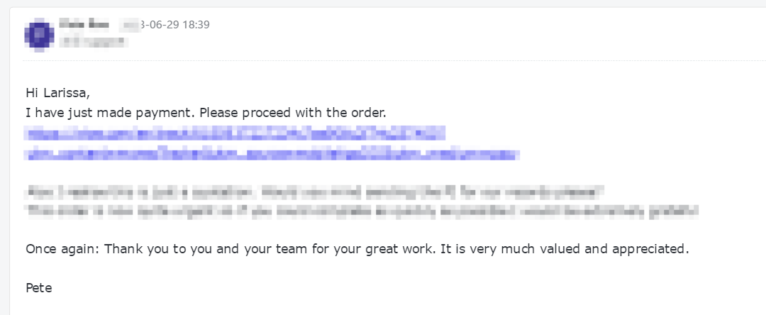
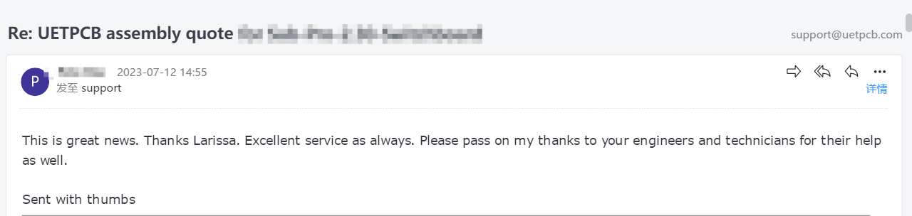
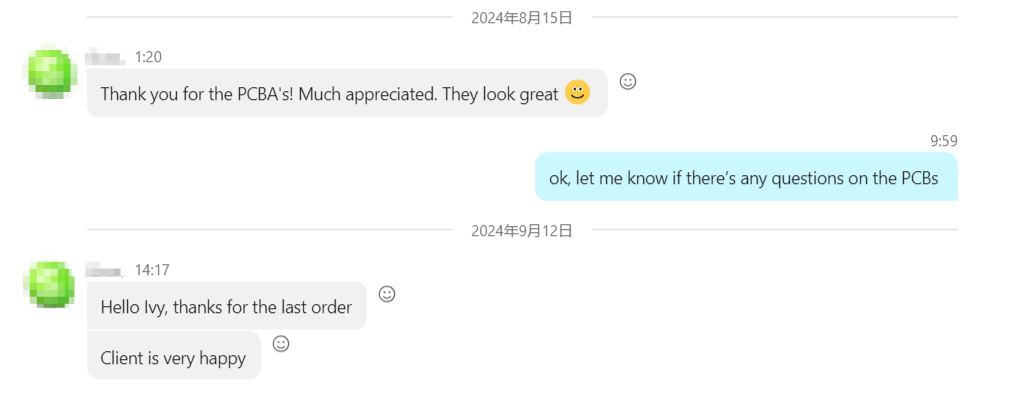
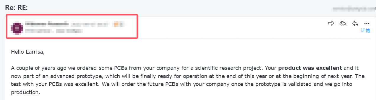
客户对我们的PCBA服务的评价

我们随时为您提供帮助

有任何问题吗?欢迎随时联系我们,我们将在24小时内回复您的咨询。

We specialize in building your pcb prototype and PCB assembly with rapid turn times.


    Please prove you are human by selecting the heart.