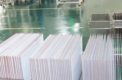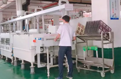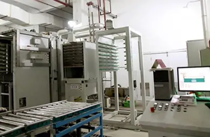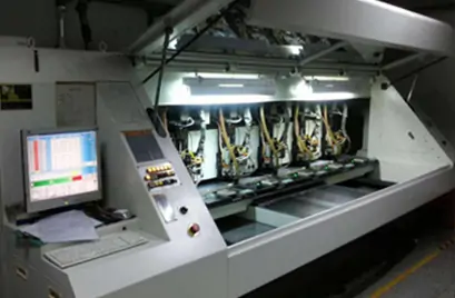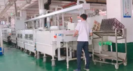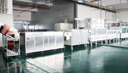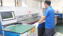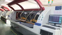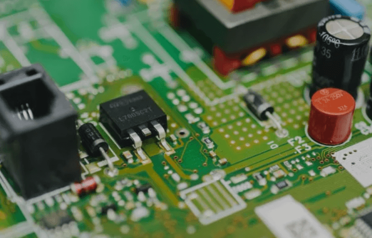
Pcb prototype service introduction
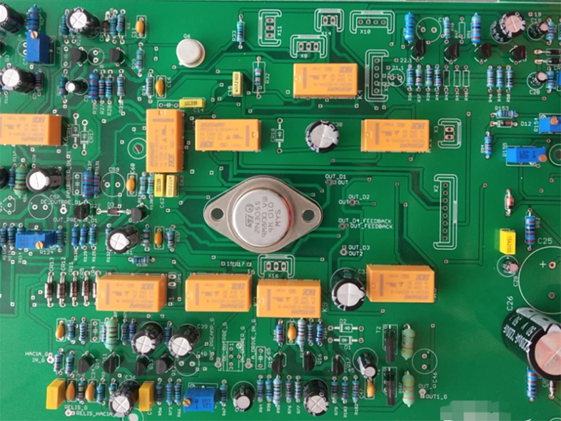
Component assembly
| 功能 | Through-Hole | SMT (Surface Mount Technology) |
|---|---|---|
| Component Type | Long-leaded, larger components (e.g., electrolytic capacitors, transformers) | Compact, leadless components (e.g., SMD resistors, ICs) |
| PCB设计 | Requires drilled holes (common for single/double-layer boards) | No drilling needed (ideal for high-density multilayer boards) |
| Mechanical Strength | High (suitable for physical stress or high-temperature environments) | Lower (relies on solder paste adhesion) |
| Cost/Efficiency | Higher labor costs (ideal for prototypes/low-volume) | Highly automated (optimized for mass production) |
Manual and automated Insertion
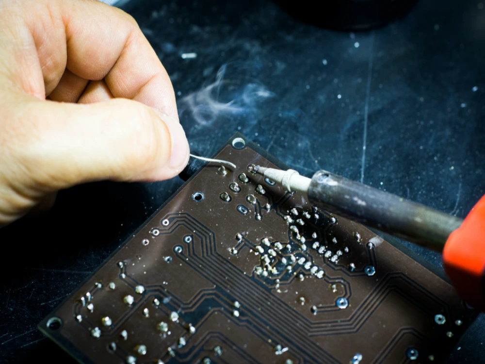
Lead-free or RoHS soldering
Double Wave Flow Solder
Selective wave soldering
Use low and high melting point solder
Conformal Coating
IC Programming
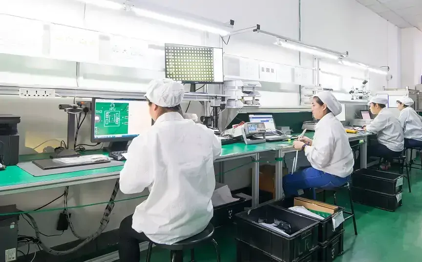
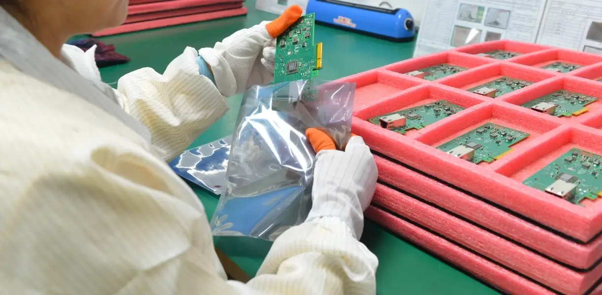
Inspection and functional testing
UETPCB 是位于深圳的专业 PCB 供应商及 PCBA 制造商。我们专注于提供高质量的 PCB 组装服务。作为一家值得信赖的 PCB 供应商,我们提供从 PCB 制造到组装的一站式服务。我们的专业团队拥有丰富的经验和专业技能,能够满足各行各业的需求。 我们的目标是成为您在中国PCBA制造领域的首选合作伙伴。如果您需要优质的PCB组装服务,请联系我们。
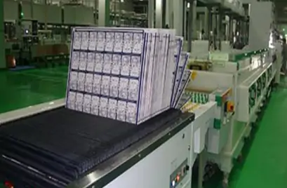
Step 1:Creating a designed layout on the copper-clad laminate
Step 2:PCB manufacturers will etch or remove excess material from inner layers to reveal images and pads.
Step 3:Laminating printed circuit board materials at high temperatures for creating the PCB layer stack up
Step 4:Creating mounting holes, through-hole pins, and vias on PCB
Step 5:Etching and removing the excess copper of the surface layer to reveal images and pads
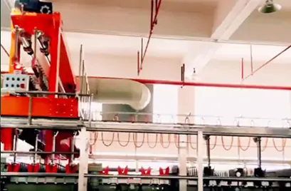
Step 6:Placing plating pin holes and via holes
Step 7:Creating a protective coating or solder masking on the surface
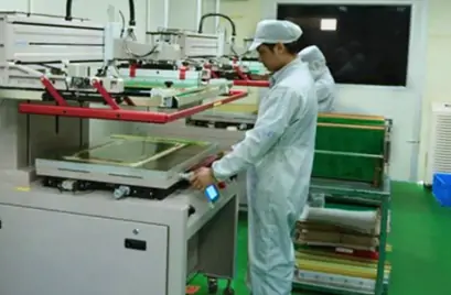
Step 7:Silkscreen printing, logos or other markings, and installing polarity indicators on the surface
有任何问题吗?欢迎随时联系我们,我们将在24小时内回复您的咨询。
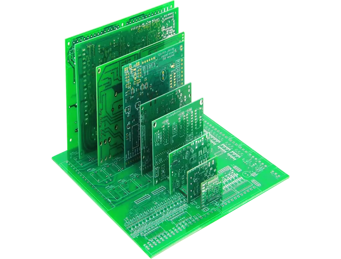
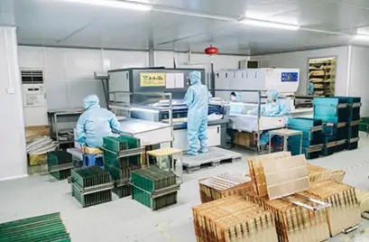
We specialize in building your pcb prototype and PCB assembly with rapid turn times.