
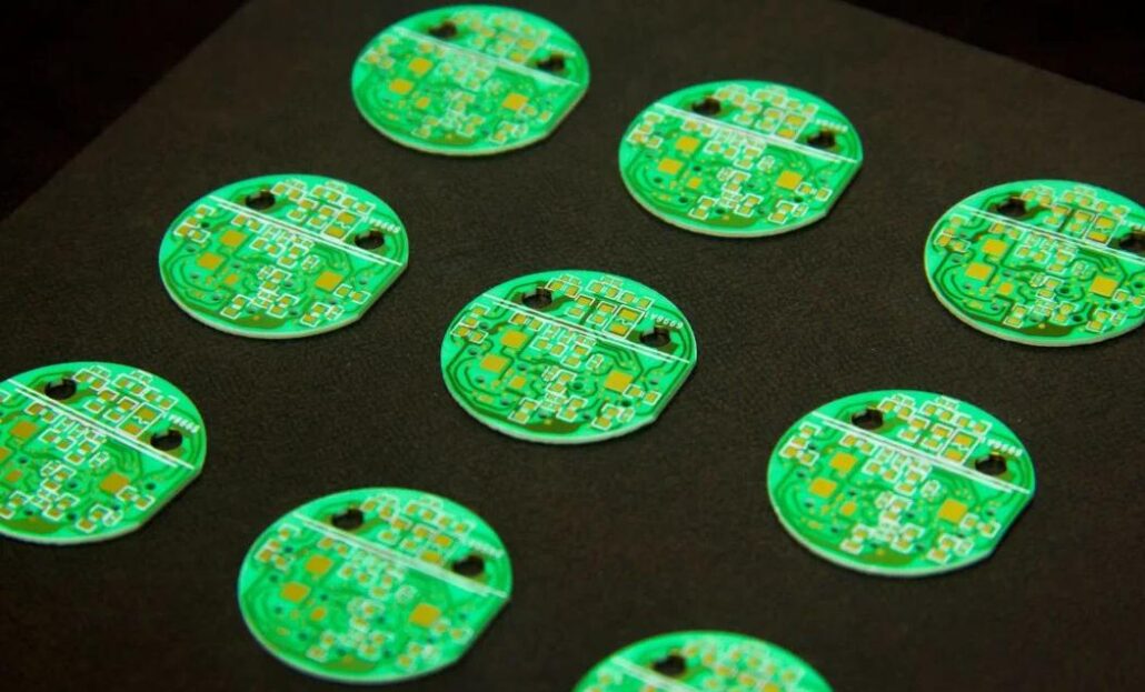
Long before printed circuit boards (PCBs) appeared in films. There were already vacuum tubes performing a similar function. At the simplest terms, PCBs are utilized for linking components in electronic goods in a hassle-free and more economical manner. Typically, PCBs are made of insulating material. Pcb’s are coated with metal, either on the bottom of…
06
5月
5月
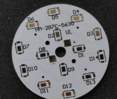
Introduction to aluminum pcb board Aluminum circuit board is the most common circuit board among metal PCBs. The aluminum substrate is a metal-based copper clad laminate with good heat dissipation function. Generally, a single panel is composed of a three-layer structure: a circuit layer (copper foil), an insulating layer, and a metal base layer. Because…
28
4月
4月
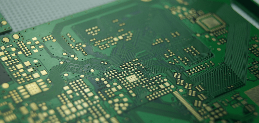
Printed circuit board (PCB) has become a part of most electronic devices today. PCB designers can create impressive boards with many features. Whether you’re a designer creating a circuit board on a personal project or a designer working on a great team, it’s important to get the design right before moving on to manufacturing, and…
20
4月
4月
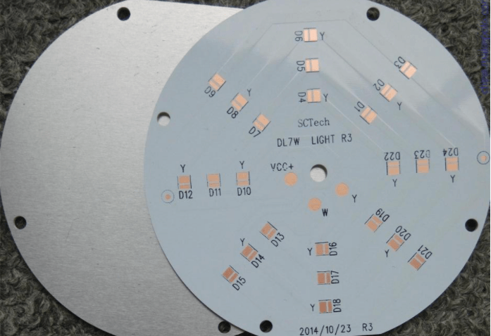
With the rapid development of the electronic industry, the size of electronic products is getting smaller and smaller, and the power density is getting larger and larger. To solve the problem of heat dissipation is a great challenge to the design of the electronic industry, and aluminum PCB is undoubtedly a good way to solve…

16
4月
4月
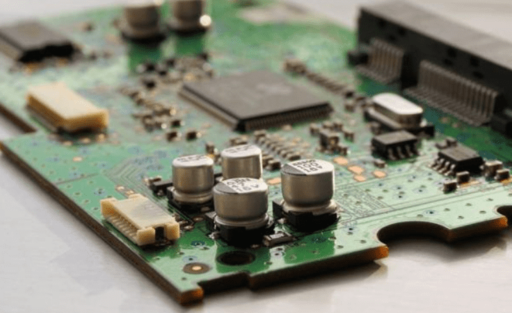
PCBA technology has become increasingly mature, played a key role in the current various intelligent equipment,It has a wide range of applications. If you want the printed circuit board to achieve the desired design function, except the hardware, the matching support of the software is very important, the program is loaded into the IC through the…
09
4月
4月
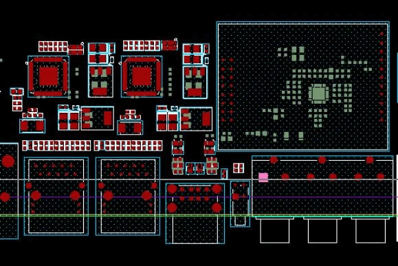
完成PCB设计后,将其发送至PCB工厂进行PCB样机制作或批量生产,随附一份PCB工艺文档,其中将说明PCB表面处理方式;不同的PCB表面处理方式,其成本及适用场景各不相同。首先,为什么我们需要对……进行特殊处理……
31
3月
3月
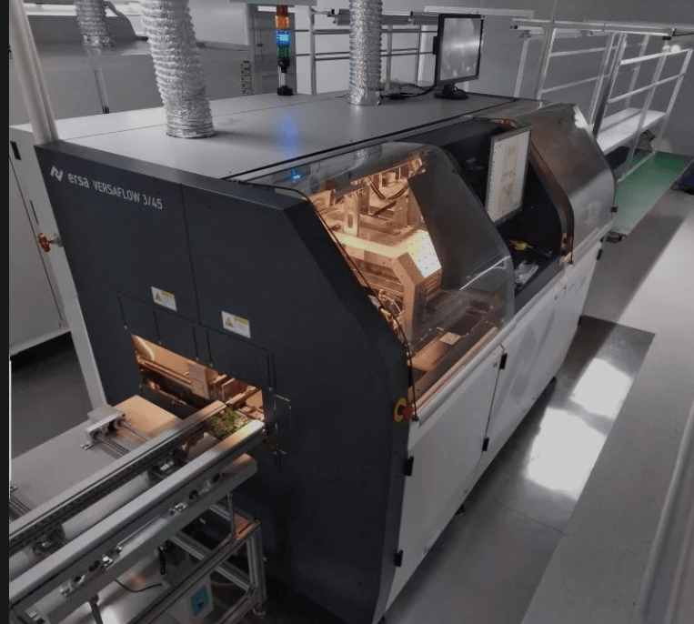
问题 原因 影响 低噪声放大器/谐振腔电路布局(接收机) 电感器方向 射频贯穿孔 退化/π型网络布局(发射机) 电感器方向 射频贯穿孔 π网络各支路间的共用接地过孔 过孔寄生参数 贯穿孔、射频泄漏 各接收器模块间的共用接地过孔 过孔寄生参数 串扰、射频贯穿、 射频泄漏 去耦电容的走线过长 高阻抗连接 去耦效果降低 元件间距过大……
29
3月
3月
波峰焊接技术简介:DIP插装和SMD粘贴工艺的专用波峰焊接是PCB组装行业中现代电子制造的重要工艺之一,尽管它已受到SMT技术的影响,但仍有相当多的电子元器件无法被SMT封装技术完全取代……
24
3月
3月
如今,电子PCBA硬件终端客户对电子代工服务的需求日益旺盛。传统的PCBA制造商由于供应能力薄弱、缺乏价格优势、供货不稳定以及劳动效率低下,导致转化率较低,并面临客户日益减少的问题。然而,在……的过程中……