
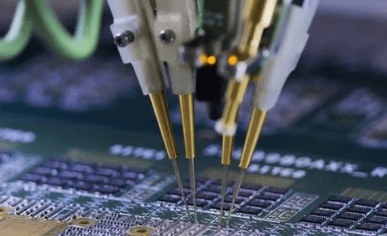
关于PCB电气测试您需要了解的内容 为何要在PCB制造过程中开始进行电气测试 在PCB板的生产过程中,很难避免由外部因素引起的短路、断路和漏电等电气缺陷。此外,PCB正不断向高密度、细间距以及……
18
8月
8月
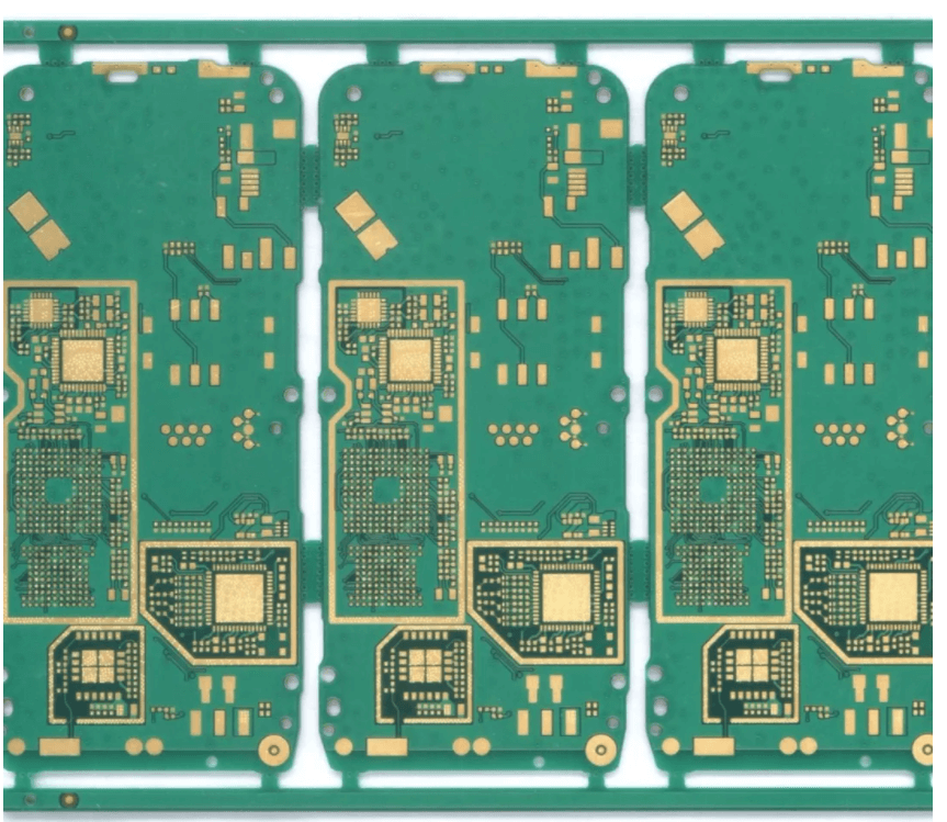
为了提高PCBA的生产效率、降低生产成本,通常会将PCB电路板进行拼板处理,以便进行电路板组装生产,这不仅能方便PCBA的焊接,还能节省时间。PCB拼板的目的是什么?提高SMT组装的效率。拼板中包含的电路板数量越多,……
05
8月
8月
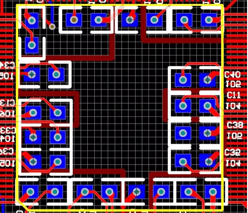
关于PCB过孔的必知知识 电路板由多层铜箔构成。电路的不同层通过孔(VIA)相互连接。电路板的作用是导电,因此这种孔被称为通孔。PCB过孔的类型 镀通孔……
30
7月
7月
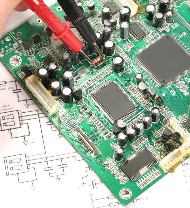
电路板的制造是一个耗时的过程,通常并不被视为“简单的事”。尽管有些爱好者只要备齐所需材料,就能在家中自制电路板,但这些自制电路板通常比机器制造的要简单一些。此外,这也会相当耗时……
12
7月
7月
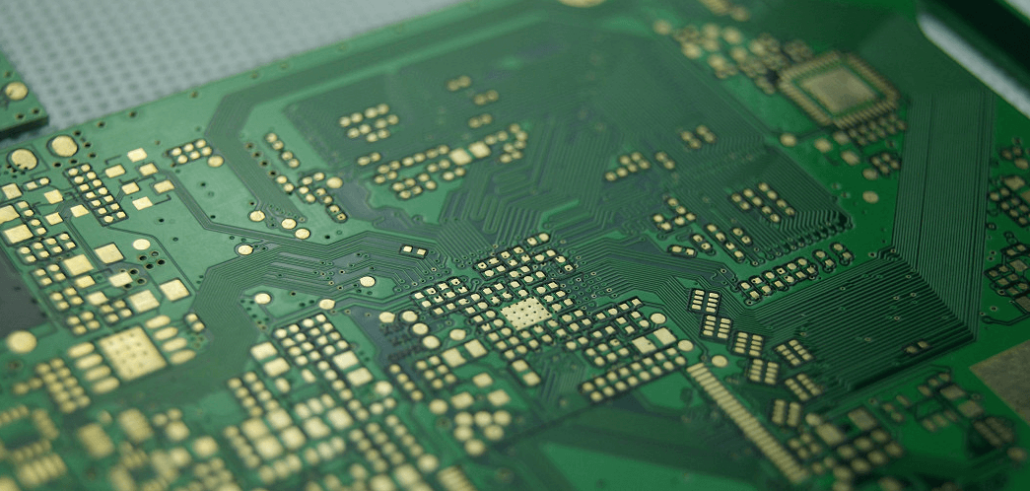
Pcb circuit boards are widely used in various industries such as electrical appliances, computers, mobile phones, and computers. It is the main part of electronic components. However, circuit boards have a powerful enemy – pcb corrosion. A circuit board that strong acids or other chemicals have corroded will not be able to continue working. Corrosion…
09
7月
7月
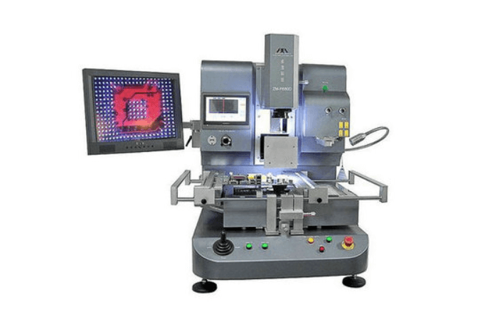
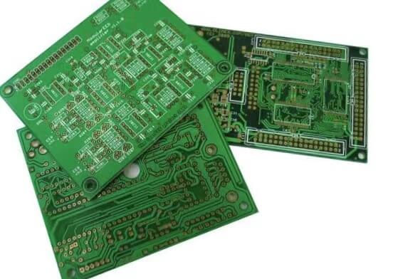
Ball grid array (BGA): The process of replacing all the solder balls on a chip’s ball grid array is called BGA rebound. BGA packages have become very popular in the printed circuit board (PCB) design and manufacturing industry. These packages help reduce the size of a PCB and improve its functionality. BGA can withstand the…
23
6月
6月
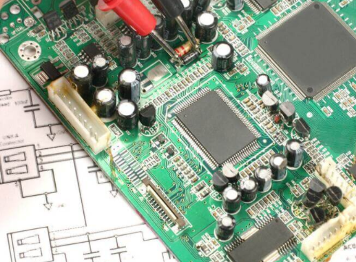
PCB designers use digital design automation to generate a design frequently. The EDA app stores layout info, facilitates editing the plan, and automates repetitive design tasks. The very first phase is converting the circuit schematic to a web list. The web listing gives component hooks and the circuit structures or baits that every pin connects….
17
6月
6月
If that’s the case, use a magnifying glass or low-power microscope. Cracks or stains in any solder ought to be noted. Assess all holes. When none-plated through holes have been given, make certain this is the situation on the plank. Poor plating through pockets can lead to a brief circuit between layers and lead to…