A 4-layer PCB is the most popular type of printed circuit board used in electronics. It consists of 4 layers with different functionalities. These boards are typically used in all general-purpose electronic gadgets. In this article, you will learn more about 4-layer PCB thickness.
Understanding 4-Layer PCB Thickness
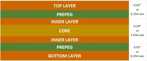
The thickness of a 4-layer PCB greatly affects its strength and functions. As you know, the thicker the PCB is, the stronger it is. Also, thicker PCBs have the advantage of efficient heat dissipation. However, four-layer PCBs are usually 1.6mm or 0.06 inches thick. The exact thickness, though, relies on the shape and the materials used.
Now, what affects the thickness of a 4-layer PCB? The first thing that affects the most is its material. For example, all regular PCBs are made of FR4 material. It is usually 1.6mm or 0.06 inches thick. The next thing is the copper layer. If you are designing a bigger board, you will need a thicker copper layer. Consecutively, the thicker copper layer adds to the overall thickness of a 4-layer PCB.
Formation of 4-Layer PCB Thickness
A 4-layer PCB has one top layer, one bottom layer, and two inner layers. Generally, the top layer keeps all the components and is used as the signal layer. On the other hand, the bottom layer also acts as the signal layer or ground.
The variations may change based on different criteria. In general, you can find three stack-up variations of a 4-layer PCB. All these stack-ups heavily affect the overall thickness of the 4-layer PCB.
Before we explain these variations, you may wonder about the connecting strategies of this layer. The components are always on top. However, you may wonder about the working principle of variation #2. The simple answer to this question is the use of vias. Vias typically connect the layers.
Stack Up Variation#1 S-P-G-S
This variation is the most common one. This structure’s top and bottom layers act as the signal layer. The second layer acts as the Power layer, while the third layer is the ground layer.
The distance between the power and ground layers is less in this variation. Therefore, your PCB experiences less impedance. This type of PCB is often used in communication devices and consumer electronics.
Stack Up Variation #2 P-S-S-G
In this variation, the top layer is the power layer, and the bottom layer is the ground layer. The inner two layers are both signal layers. Since the distance between the power and bottom layers is bigger, the impedance is higher for these PCBs. This type of PCB is often used in power supplies and industrial control systems.
Stack Up Variation #3 S-G-P-S
This variation is almost the same as variation #1. The only difference is in the position of the ground and power layers. However, the primary signal layer is always on top. Since the ground and power layers are apart, the impedance is lower.
How Much Does a 4-Layer PCB Cost?
A typical 100x100mm 4-layer PCB costs around $100 to $500 for 100 pcs. The cost may change if you choose a more complex design and rare components. However, this cost generally depends on several factors.
First, it counts the material quantity. You must order quantity from 5 pcs or more. Some factories fix the minimum amount to be at least 100 pcs. Next, you should check the size and thickness of the board. More extensive and thicker PCBs cost more. Next, the complexity of the design and engineering support adds to the cost. Finally, the delivery and shipping conclude the overall costs.
Sum UP!
A 4-layer PCB is a common and general-purpose PCB. The thickness of these PCBs generally ranges from 1.6mm to 3.2mm. If you are looking for high-quality 4-layer PCBs, contact us today. We have a professional team of experts who are always happy to help.


