
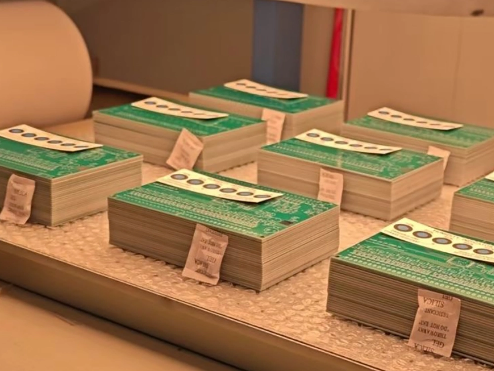
Multilayer PCB Manufacturing Services
UETPCB is an expert PCB supplier. We’ve spent years perfecting our multilayer PCBs, from buying the parts to testing them. We always adhere to IPC level 3, RoHS, and ISO9001:2008 standards.
- 1. One-stop service: one-stop processing from PCB prototyping to SMT placement.
- 2. Speedy: fast quotation and quick response
- 3. Fast delivery: over 98% on-time delivery rate
- 4. High flexibility: various parameters can be customized
- 5. Good service: professional customer service, giving the best solution
- 6. Quality assurance: 100% AOI & E-Testing, CoC provided.
- 7. Big offer: PCBA prototyping minimum $50, PCB minimum $5
Our Multilayer PCB Fabrication Capability
| Feature | Specification |
|---|---|
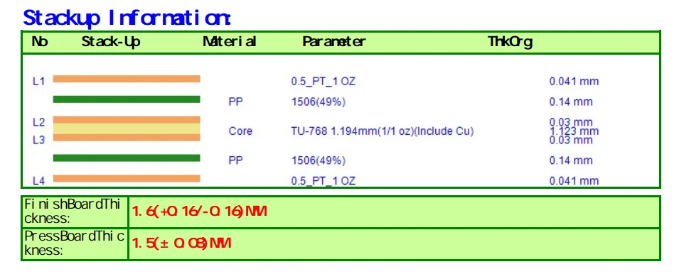
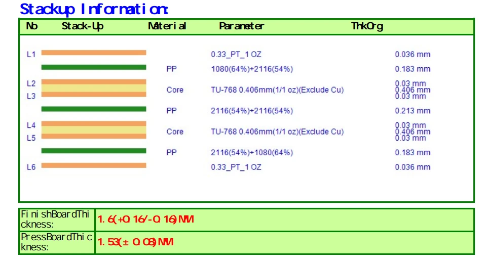
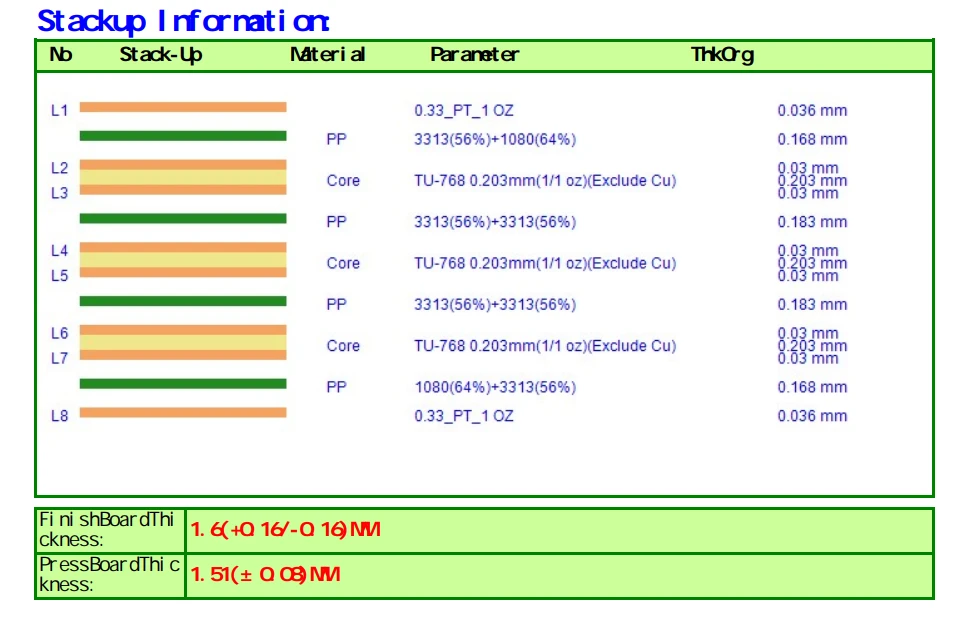
| Number of layers | 4-48 layers |
| PCB thickness | 0.1-10.0mm |
| Maximum board size | 800*950mm |
| Minimum line width and spacing | 2/2mil |
| Min. through hole (Mechanical) | 0.15mm |
| Min. finished hole (laser hole) | 0.076mm |
| Max Aspect Ratio | 20:1 |
| Inner layer copper thickness | 8oz |
| Outer layer copper thickness | 8oz |
| Impedance Control Tolerance | 5% |
| Min. distance between the IC pads | 8mil |
| Min. SM bridge for green solder mask | 3mil |
| Min. SM bridge for black solder mask | 4mil |
| PCB type | Ridid, FPC, Rigid-flex, Metal base, Copper base |
| PCB Materials | FR4, High TG, Halogen Free, High Frequency, High Speed |
| Solder Mask Color | Green, Blue, Red, White, Black, Yellow, Matt green, Matt black |
| Surface Treatment | HASL, ENIG, OSP, GOLD PLATING, IMMERSION Ag, IMMERSION Sn |
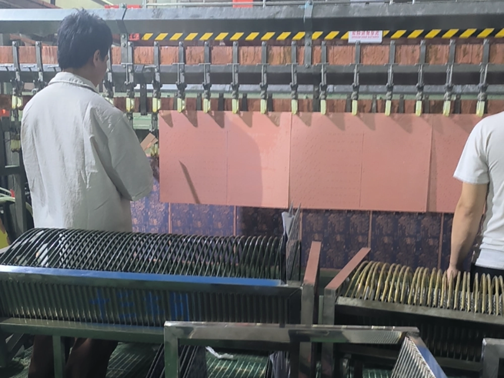
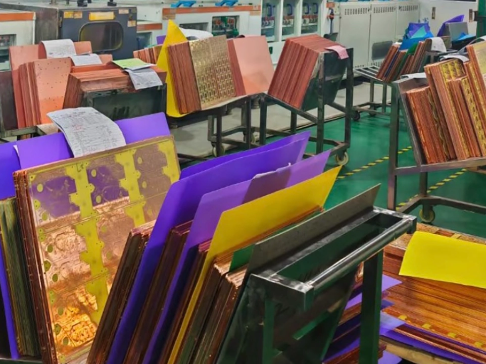
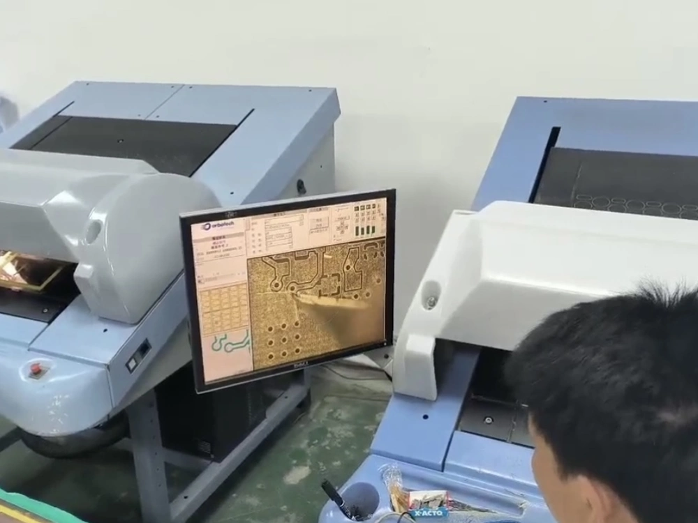
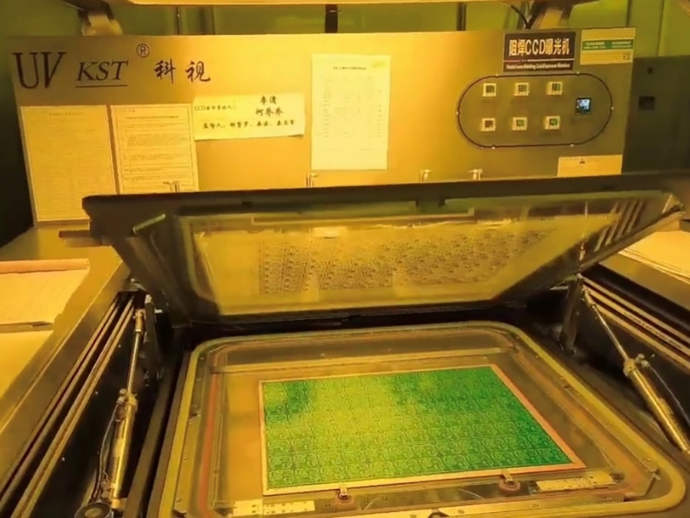
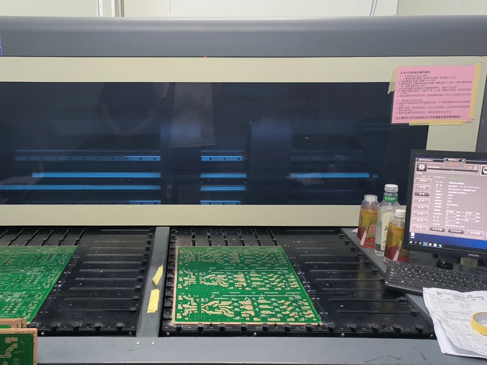
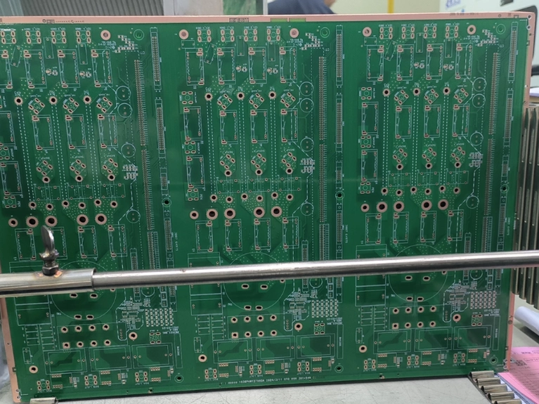
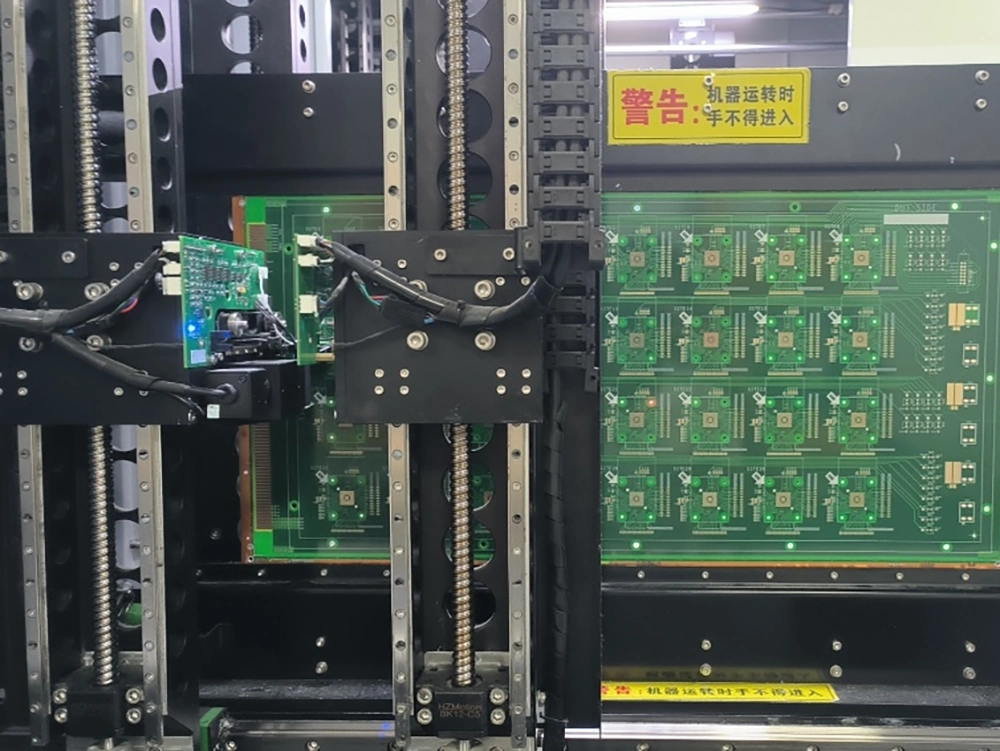
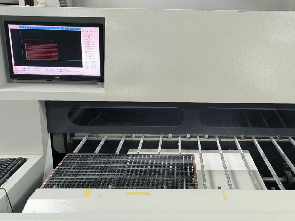
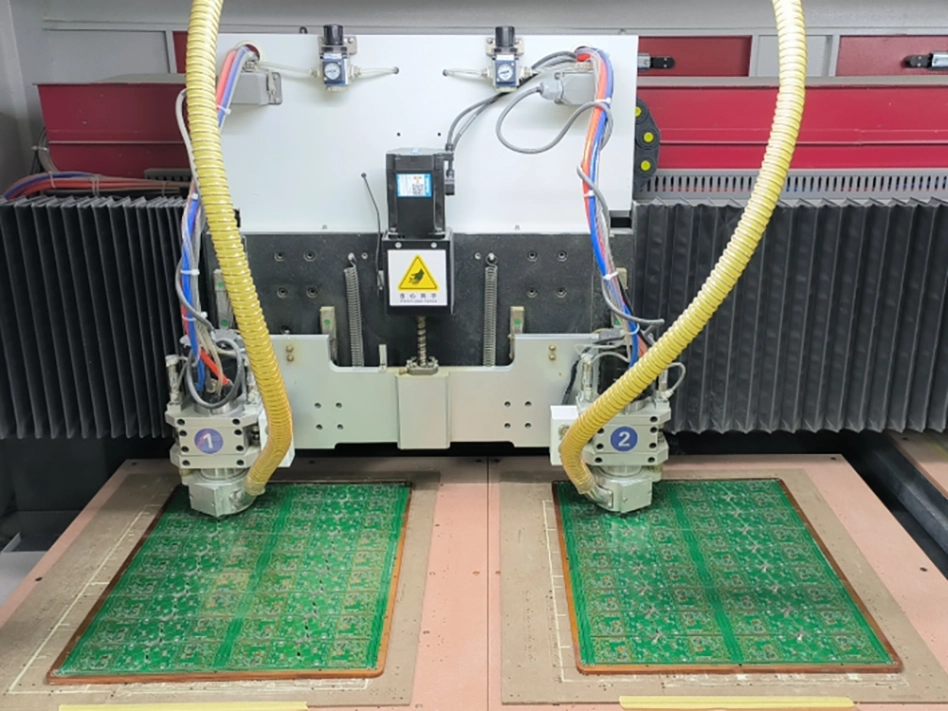
Multilayer PCB Manufacturing Process
In making multilayer PCBs, we pay close attention to every step to make sure they are top-notch.
We start by designing where the circuits will go, then drill holes for the parts to fit in. We keep a close eye on each stage to ensure the PCBs work well for all kinds of electronic gadgets.
You can trust our process because making high-quality PCBs for our customers is what we’re all about. Here’s how we do it:
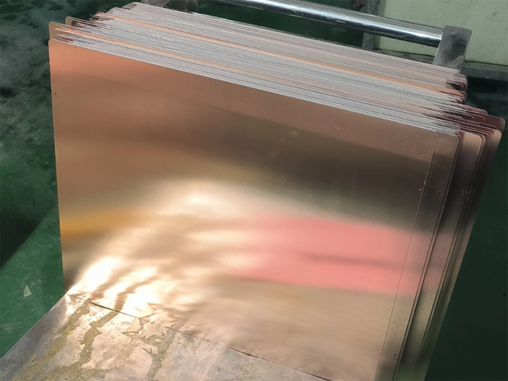
1. Board Cutting
2. Drilling
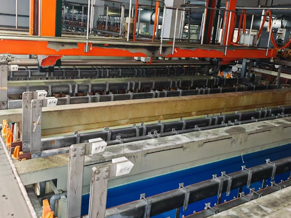
3. Electroless Copper Deposition
4. Copper Plating
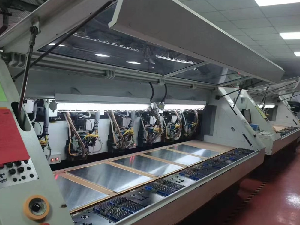
5. Circuit Printing
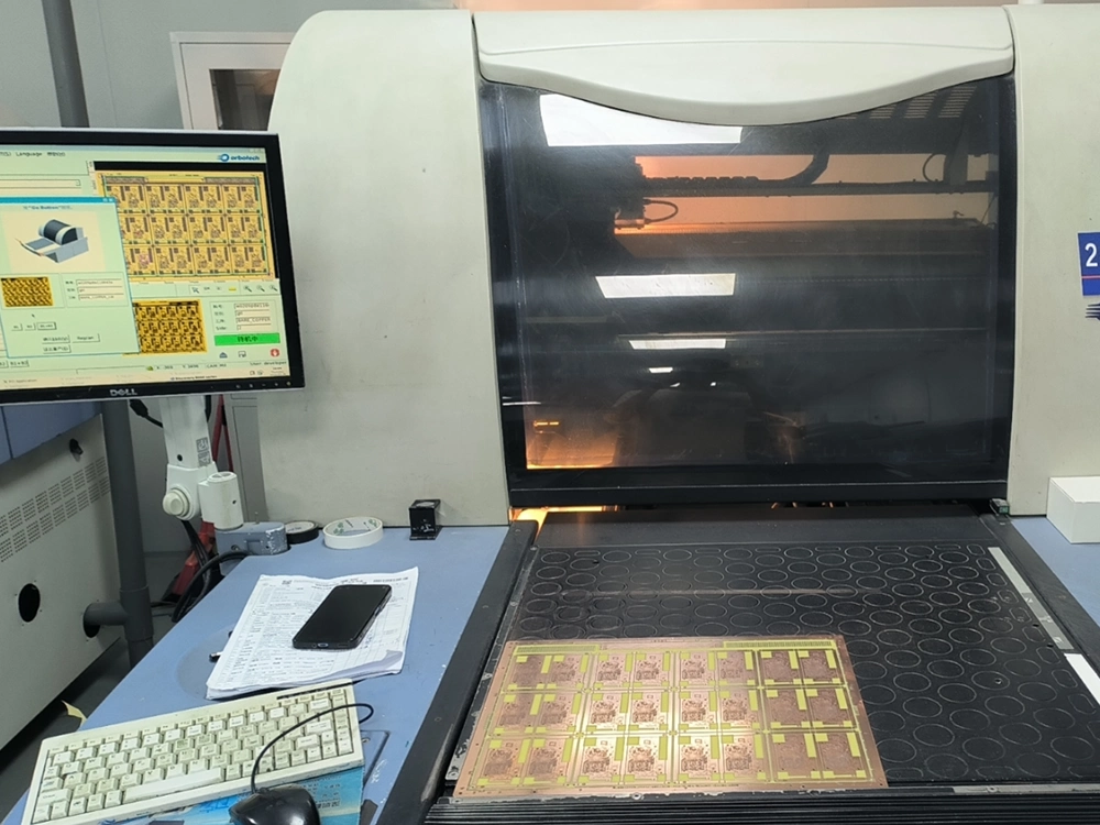
6. AOI
7. PCB Maintain
8. Solder Mask
9. Silkscreen
10. Surface Finish
11. Electrical Test
12. V-Scoring
13. PCB Milling
14. Final Inspection
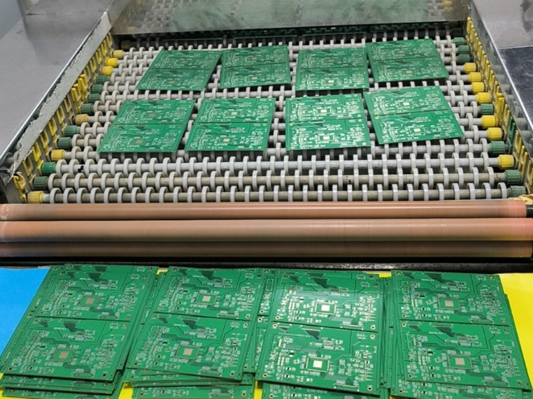
15. PCB Cleaning
16. Packaging
Advantages Of Multilayer PCB Over Single and Double Layer PCB
All of these PCBs are good choices. How you decide to go with a multilayer or single-layer structure depends on what type of product you need to produce. Essentially, if you want to produce complex devices that are small, lightweight, and require high quality, a multilayer PCB may be your best choice. However, if size and weight are not important factors in your product design, a Single or Double Sided PCB design may be more cost effective.
Lighter weight:
Integrating components in a multilayer PCB means less need for connectors and other details, which can provide a lightweight solution for applications. Its can accomplish the same amount of work as multiple single-layer PCBs but smaller. This is because multilayer pcb fabrication require fewer connected components, which reduces weight. This is an essential consideration for smaller electronics where weight is a concern.
Higher assembly density:
Multilayer pcb fabrication allows greater functionality, capacity, and speed with increased thickness.
Smaller size:
In general, a single-layer pcb has a little more area. Because it must increase the surface area of the circuit by increasing its size, it is better suited for use in devices with large volumes and few functions.
Enhanced design features:
Overall, multilayer PCBs outperform typical single-layer PCBs. More controlled impedance characteristics can achieve more substantial EMI shielding and improve overall design quality.
Application demonstration of multilayer PCB
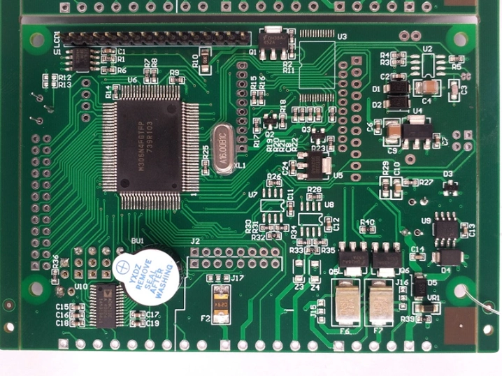
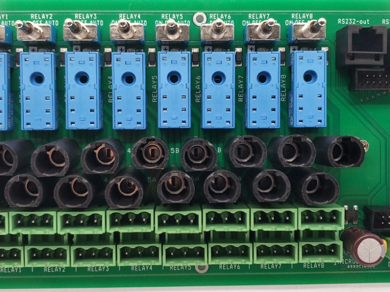
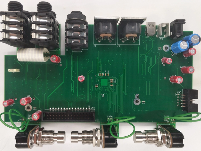
Smart Home PCB
Industrial Control PCB
Medical Electronics PCB
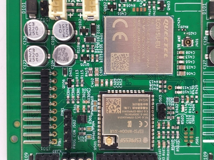
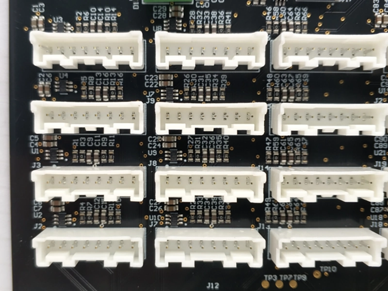
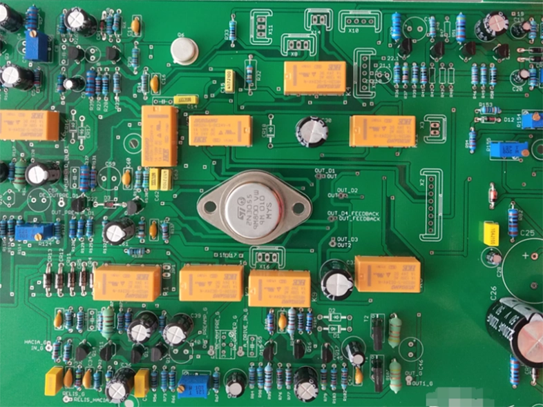
Navigation motherboard PCB
Automotive Electronics PCB
PCBA for Security Industry
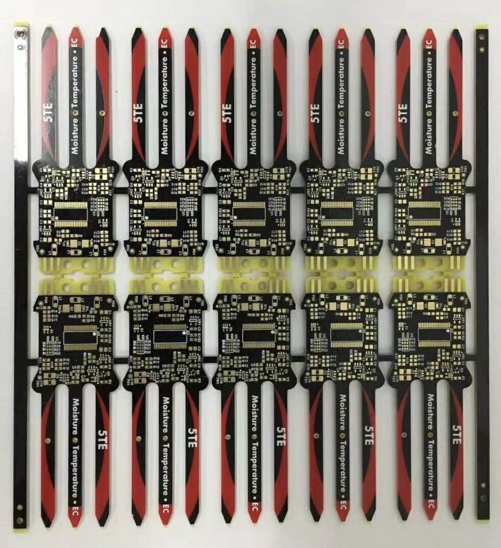
Industrial Control Signal Processing Board
Communication Equipment PCB
Power Inverter Motherboard
How Many Layers Can A PCB Have?
We support 4-48 layers multilayer pcb fabrication.
Why Do PCBs Have Multilayer PCB Circuit Board?
Multilayer boards have emerged with the development of the electronics industry. Because there is some advanced equipment, single-sided or double-sided PCB can not meet. Multilayer boards is lighter, smaller, and features higher operation speed than traditional printed circuit boards. All the advantages make them appropriate to be used in high-end electronic equipment like handheld devices, test equipment, heart monitors, etc.
And the preference for multilayer circuit board is still largely dependent on industry trends. Electronics continue to move toward versatility and are small, thin, and lightweight. So single and double sided PCBs can no longer meet the changing needs. And their ability to balance size and functionality has proven limited, but multilayer PCBs offer a comprehensive solution.
While there are several drawbacks to using multilayer boards, such as increased cost, design time, and production investment, these costs are increasingly accepted in today’s world. Functionality is largely favored over price, and people are willing to pay more for high-capacity electronics. In addition, as technology becomes more mainstream, production techniques and machines will eventually become cheaper, especially as new technologies enter the industry.
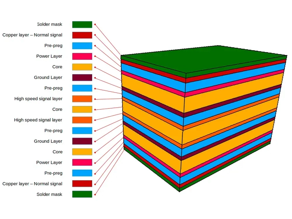
What Is Multilayer PCBs?
Multilayer PCBs feature three or more layers of conductive copper foil buried in several layers. It is laminated and glued between each layer with a thermally protective insulating layer. It finally appears as a double-sided circuit board with several layers. Multilayer boards have various through-holes for all electrical connections. These types of vias include blind and buried vias and plated vias. This is the simple definition of multilayer boards.
Advantages and Disadvantages of Multilayer PCBs
Compared with single-sided or double-sided PCBs, multilayer boards have higher assembly density, flexibility.
Advantages:
High efficiency: Its enable more advanced design, manufacturing, and assembly techniques. So their inherent electrical characteristics allow them to achieve greater capacity and speed.
High Durability: Its use multiple layers of insulation between circuit layers. They are bonded together using prepreg adhesives and protective materials, making them more durable than standard PCBs.
Smaller size and lighter weight: Its use stacking and lamination techniques, resulting in smaller and lighter weight boards. This is one of its most prominent and highly acclaimed benefits.
Single connection point: Its use a single connection point that can be designed to work together on a board. This particular design simplifies the complex design of electronic devices and reduces size and weight.
Disadvantage:
High cost: Making a multilayer board is much higher than that of a regular pcb. Because multilayer pcb manufacturing machines are very expensive, it is still a relatively new technology.
Narrow application range: Multilayer pcb fabrication requires specialized multilayer pcb manufacturing machines, which not all multilayer pcb suppliers have the funds or need.
Long production time: Each board of a multilayer pcb fabrication requires a lot of time, which leads to more labor costs.
We’re Here To Help You
Any questions? Contact us anytime, and we’ll respond to your inquiries within 24 hours.