
HDI PCB Definition
HDI boards are defined as printed circuit boards that pack more circuits into a smaller area compared to standard PCBs. There are several types of HDI boards:
- 1.type I
- 2. type II
- 3. type III
Each types with different features as outlined in the IPC-2226 standard.
Please reach out if you need more information or help. We’re here to assist you!
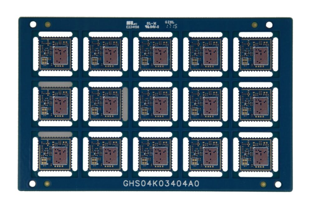
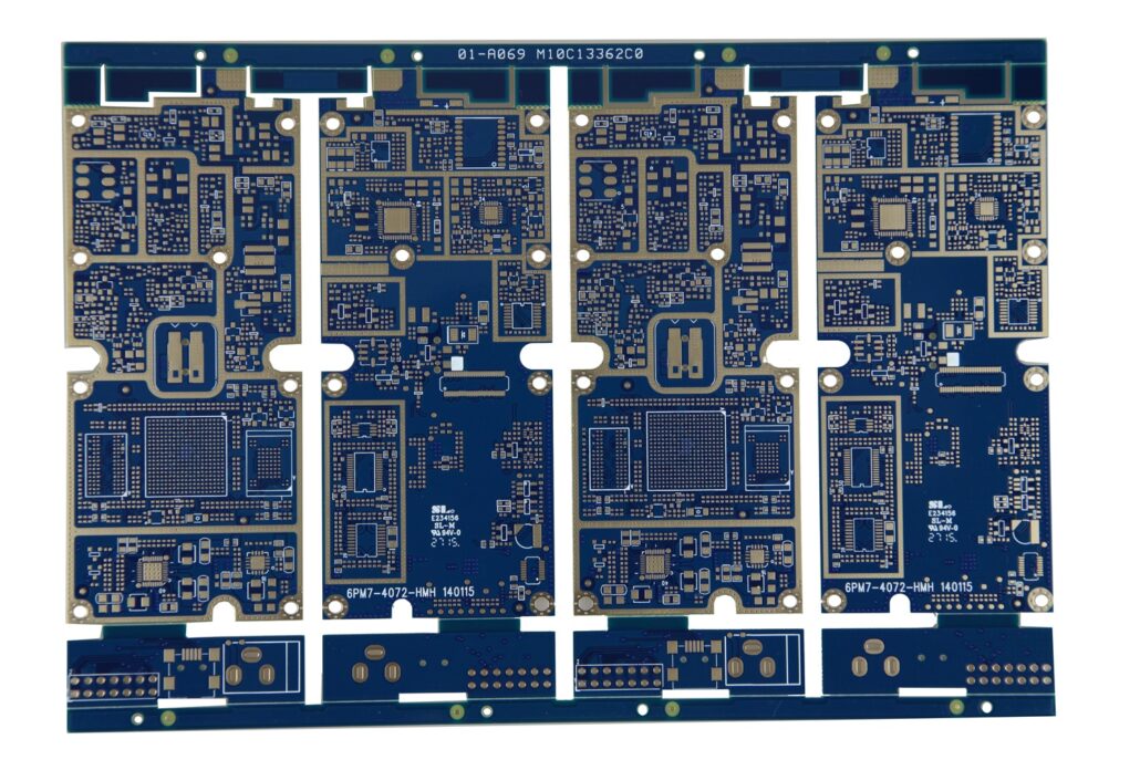
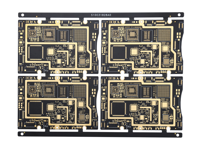
Our HDI PCB Capability
| Feature | specification |
|---|---|
| Number of layers | 4 – 22 layers standard, 30 layers advanced |
| Technology | Multilayer PCBs have denser connection pads than standard boards. They include finer lines and spaces. The boards also feature smaller holes and capture pads. This design allows micro vias to penetrate select layers and integrate into surface pads |
| HDI builds | 1+N+1, 2+N+2, 3+N+3,4+N+4, any layer / ELIC, Ultra HDI in R&D |
| Materials | FR4 standard, FR4 high performance, Halogen free FR4, Rogers |
| Copper weights (finished) | 18μm – 70μm |
| Minimum track and gap | 0.075mm / 0.075mm |
| PCB thickness | 0.40mm – 10.0mm |
| Maxmimum dimensions | 800mm x 950mm; dependant upon laser drilling machine |
| Surface finishes available | OSP, ENIG, Immersion tin, Immersion silver, Electrolytic gold, Gold fingers |
| Minimum mechanical drill | 0.15mm |
| Minimum laser drill | 0.10mm standard, 0.075mm advanced |
HDI PCB Design
The process of HDI PCB design consists of these main steps:

Requirements Analysis
The performance requirements must be spelled out first. These include the size constraints and board cost targets.
Schematic Design
Design the circuit connections; figure out how components are linked.

PCB Layout
Translate circuit schematics into specific PCB design drawings. At this stage, we need to place components and optimize routing for electrical performance to minimize signal interference.
Via Hole (Vias) Configuration
Via hole technology is critical in HDI PCB design, so decide on via hole sizes and locations to support multi-layer connections.

Simulation Testing
Electronic simulation tests a design before it is manufactured and checks whether or not it is valid and performs as expected within a system.
Prototype Manufacturing
Make PCB prototypes based on design drawings – this part verifies theory through practice.

Testing & Debugging
Test the prototype board’s functionality and speed, adjusting where necessary to fix design errors.

Mass Production
Start mass production once the prototype has been checked and found correct.


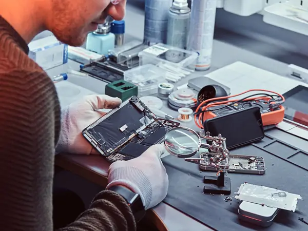
Our HDI PCB Technology
HDI technology is a high-end technology used to manufacture HDI PCBs. This printed circuit board features high density and exemplary performance in circuit interconnection.
According to the vias, HDI boards can be divided into six different types:
- ⚫ Face-to-face through vias
- ⚫ Through vias and buried vias
- ⚫ Two or more layers with through vias
- ⚫ Non-electrical connection and passive substrate
- ⚫ Coreless construction with layer pairs
- ⚫ Alternate constructions of coreless constructions with layer pairs
- ⚫ HDI Printed Circuit Board Manufacturing
Advanced HDI Technology Methods
- Via in-pad process:
In this process, HDI PCB manufacturers place bias on the surface of the flat lands. Then, they fill the vias with conductive or non-conductive epoxy. Later, they are capped and plated over, making the via invisible. - Via fill technology:
Specific materials include silver-filled, conductive epoxy, non-conductive epoxy, electrochemical plating, and copper-filled. - Non-conventional HDI PCB building:
HDI PCBs must combine more lines and annular rings on a thin, high-density board. - Laser drill technology:
A laser beam 20 microns in diameter can create the smallest vias on the surface of HDI PCBs. This high-energy light is precise and efficient and can cut through metal and glass to make a tiny hole.
HDI PCB Application & Advantages
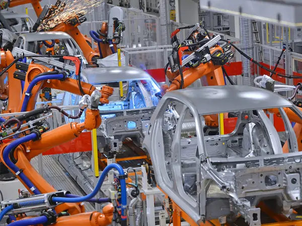
Though HDI PCB has a complex manufacturing process, it has a wide range of applications. It can be used in various industries, such as electronics and medical. The lighter weight and small size give it appropriate reasons to be installed in miniature equipment.
HDI PCB is consumer-driven and fit for more delicate and sophisticated electronic equipment. Nowadays, people prefer agility electronic equipment because of its convenience and lightweight. HDI PCB makes the equipment small and smart. It is thin, light, and features high-end technology and high-speed operation capability.


Your Reliable HDI PCB Manufacturing
High-density interconnection technology
Our HDI PCB uses high-density interconnections, which allow it to support many more electrical connections in a limited area.
High-quality materials and manufacturing processes
We use the best materials and most advanced techniques. We also ensure that HDI PCBs perform at a top level of electrical performance.

Customized services
Here, we offer you custom solutions for HDI PCB. We tailor-make our designs and manufacturing to fit what you want them to be like.

Fast delivery and quality service
We have streamlined production processes. What’s more, we work with professional teams that guarantee you get the best quality HDI PCBs.
We’re Here To Help You
Any questions? Contact us anytime, and we’ll respond to your inquiries within 24 hours.