
What Is A Double Sided PCB
A double-sided PCB is a critical PCB board used in electronic manufacturing.
Double-sided PCB is an acronym for double-sided printed circuit board. Path paths and line holes in these PCBs can connect electrically to various electronic components.
Moreover, we can use double-sided circuit boards for electronic communication equipment. These PCBs have high requirements. They use advanced instruments. This ensures good performance in computers. The board is often perforated in the middle to join a double-sided PCB.
The manufacturing process of double-sided PCBs differs from that of ordinary PCBs. They have an additional copper precipitation process, which turns on the double-sided circuit. Its biodegradable mesh bags will meet all your requirements.
| Feature | Technical specification |
|---|---|
| layers | 2 |
| Technology highlights | Epoxy glass insulating materials layered with copper cladding of different thicknesses. |
| Materials | FR-4 standard, FR-4 high performance, FR-4 halogen-free. |
| Copper weights (finished) | (18 – 210)μm, advanced 1050μm / 30oz |
| Minimum track and gap | 0.10mm / 0.10mm |
| PCB thickness | 0.40mm – 3.2mm |
| Maxmimum dimensions | 510mm x 650mm |
| Surface finishes available | HASL (SnPb), LF HASL (SnNiCu), OSP, ENIG, Immersion tin, Immersion silver, Electrolytic gold, Gold fingers |
| Minimum mechanical drill | 0.30mm standard, 0.20mm advanced |
Advantages of Double Sided PCBs
A double-sided PCB board is a high-tech printed circuit board. It features two conductive copper layers on both sides, allowing it to print electrical components on both sides. Double-sided PCBs allow for more OK circuit routing. This occurs in electrical applications, leading to a higher usage rate than single-sided PCBs.
Increased design flexibility
Double-sided PCBs allow for more complex circuit designs and routing options compared to single-sided PCBs.
Higher component density
With two layers of copper traces, you can fit more components onto the PCB, making it more compact and efficient.
Improved signal integrity
Double-sided PCBs can help reduce electromagnetic interference (EMI) and signal crosstalk, leading to better overall performance.
Enhanced thermal management
The additional copper layer helps in dissipating heat more effectively, which is crucial for high-power applications.
Applications of Double Sided PCBs
Double-sided circuit boards are now an essential component of electronic equipment. People’s demand for electronic devices has risen as technology has advanced.
Ultimately, it raises the need for circuit boards. Many electrical gadgets now employ double-sided printed circuit boards (PCBs). For example, mobile phones, electronic toys, and domestic appliances are notable.
Double-sided PCB boards are critical in the mass production of fixed circuits. They additionally assist in the optimization of electrical equipment arrangement. Our most common everyday applications for double blade PCBs are ARE, APPLICATIONS, UPS SYSTEMS, and others.

Consumer Electronics
Double-sided PCBs are widely used in smartphones, tablets, laptops, and cameras.

Industrial Controls
Double-sided PCBs are utilized in various industrial control systems, automation equipment, and machinery.

Telecommunications
PCBs are essential components in telecommunications equipment. They are double-sided and used in routers, modems, and switches.

Automotive Electronics
Automakers use double-sided PCBs in cars. They are for engine control units, infotainment systems, and safety features.

Medical Devices
Double-sided PCBs are found in medical devices like patient monitoring systems, diagnostic equipment, and imaging devices.

LED Lighting
Double-sided PCBs are commonly used in residential, commercial, and industrial lighting fixtures.

Power Supplies
Double-sided PCBs are key to efficient energy management. They are used in power supply units, inverters, and converters.

Security Systems
Double-sided PCBs are employed in security cameras, access control, and alarm systems.

Gaming Consoles
Double-sided PCBs are utilized in gaming consoles for processing power and connectivity.

Aerospace and Defense
Double-sided PCBs are crucial in aerospace and defense. They are used for radar systems, avionics, and communication equipment.
Difference Between Double Sided PCB and Single Sided PCB
Single-sided PCBs have parts and traces on only one side of the board. This limits design complexity and component density. Double-sided PCBs have components and traces on both sides. They offer more design flexibility, higher component density, and better performance. But they cost more to make.
Layering
Copper traces and components are on only one side of a single-sided PCB, while they are on both sides of a double-sided PCB.
Component Density
Double-sided PCBs can fit more components and circuitry. This is due to the extra layer of copper. In contrast, single-sided PCBs have limits on component density.
Complexity
Double-sided PCBs allow for complex circuit designs and routing options. This makes them suitable for advanced electronic projects. Single-sided PCBs are more straightforward and ideal for simpler designs.
Cost
Generally, double-sided PCBs are pricier to make than single-sided ones. This is due to the extra layer of copper and more complex process.
Performance
Double-sided PCBs can offer better signal integrity and less EMI. They also have improved heat management. This makes them better for high-performance uses than single-sided PCBs.
Routing
Double-sided PCBs offer more flexibility. They allow routing traces and connections between components on both sides of the board. Single-sided PCBs have limits on routing options.
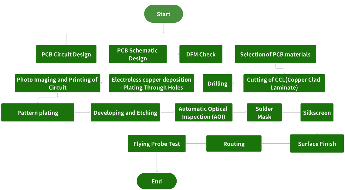
Double Layer PCB Production Manufacturing Process
First, we must prepare the tools and materials to make double-sided circuit boards. The primary materials include double-sided copper-clad heat transfer paper and sandpaper. We also need scissors, an oily pen, hydrochloric acid, hydrogen peroxide, a hand drill, and a soldering iron. Moreover, we may need a twisted pair, paper tape, soldering iron, solder, rosin, and others.
The outer and inner layers combine to make a double-sided PCB board. The following mostly explains the fabrication process for the outer layer of a double-sided circuit board.
Copper plating is the first stage in manufacturing the outer layer of the circuit board’s copper processing. In the second step, the circuit is etched, and then the tin-plated is peeled off. Ultimately, the fabrication of the outer circuit is done.
Typically, industrial staff employ two ways: “Braking Optical Inspection CCD And Laser.” The first approach uses reflection effects to determine whether a short circuit exists. The second way utilizes laser AOI. After reflecting on the copper surface, it generates varied fluorescence intensities. The second way is to evaluate a short course of reflection.
We’re Here To Help You
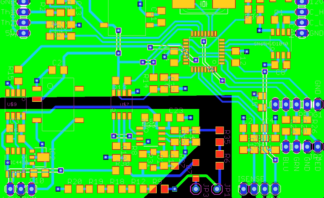
All double-sided PCBs include two copper circuit protection layers on each side for further protection. PCB designers developed the layout of double-sided PCB boards based on single-sided PCB boards. Through-hole routing is an option for both the top and bottom circuit boards. Besides, the lines can close in on each other, and we can add new lines.
To better understand our products and services, feel free to contact our customer service team at any time. We look forward to establishing contact with you, solving your needs, and creating wonderful cooperation opportunities together!