
Two important characteristics of PCB manufacturing are quality and cost. In the early days, it was almost impossible to achieve both characteristics. The introduction of automation in PCB manufacturing in the 1950s and 60s paved the way for consistent quality and reduced costs of mass-produced PCBs.
UET PCB is an experienced manufacturer of PCB assemblies. The company is dedicated to maintaining consistent quality while keeping costs affordable.
A Brief Look at Quality and Cost Savings in the PCB Assembly Process
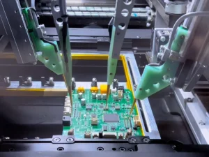
Manufacturers achieved even more cost savings when multilayer and SMT technology were introduced in the 1980’s. These processes allowed smaller PCB form factors with more wiring density.
At the turn of the new millennium (2000), East Asian manufacturers, especially Chinese manufacturers, achieved even greater cost savings. Their government supported them with subsidies, making them a global manufacturing hub. As a result, many foreign companies established remote manufacturing firms in China.
There are several key strategies and steps in making a quality PCB. However, there are also key steps in making the PCBs more affordable.
PCB Design Process for Quality and Cost Savings
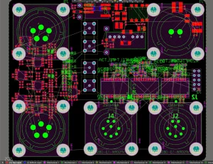
Pick a Standard Board Size
Having a standard board size can help PCB manufacturers automate the manufacturing process more effectively. If you’ll notice, both standard and minimum board sizes economize the process. It’s best to calculate both time and cost budgets in advance if you want to manufacture a non-standard board size.
Choose Economic Board Stackup
Choose an economic board stackup for significant cost savings. Usually, adding more PCB layers means having a more expensive board. A double-sided multilayer FR4 PCB can offer significant cost savings because it’s easier to manufacture and the lamination process is much simpler. If you opt for 4, 6, or more layers, prepare to calculate the cost beforehand before proceeding with your project.
Space Saving Component Placement
Before wiring, a well-thought-out component placement will make the layout easier and faster to accomplish. This method can save significant engineering time. Additionally, keeping the component uniformly aligned can help the pick-and-place machine complete its task more quickly. Keeping components on a single layer (top or bottom) will always keep assembly costs down.
Space Saving PCB Layout
A professionally made PCB layout should be optimized for space. Most of the routes should have the shortest path. Failure to do so can make your wirings longer, hence wasting precious board area.
Choose Economic Via
Choosing economic via technology can give you significant cost savings. Standard time-tested through-hole vias are always a good option. However, compared to more expensive via technologies such as micro vias, laser-drilled vias, blind vias, or buried vias, through-hole vias typically occupy more area. With this in mind, it’s important to implement efficient routing techniques.
Components Sourcing Process for Quality and Cost Savings
Another area for cost savings while aiming for quality is careful component sourcing. You must definitely source components from reliable distributors/sources, but at the same time, factor in cost. There are two methods you can choose from in sourcing your components:
| Component Sourcing Method | What it is | Advantages/Disadvantages |
| Turn-Key | Letting your PCB fabricator do the component sourcing for you. | Faster project turnaround. Cost savings for small to medium projects. |
| Consignment | You source the components yourself and then send them to your fabricator | You may encounter logistics overhead, although there are significant cost savings at scale. |
PCB Manufacturing Process for Quality and Cost Savings
Cost-Effective Surface Finish
If your project does not need special connectors, fine-pitch components, or BGAs, you can opt for the time-tested HASL surface finish. HASL stands for Hot Air Solder Leveling. However, if you have special needs, you may have to opt for the other types. Below is a table you can check for surface finishes:
| Surface Finish | Costing | Description |
| HASL (Hot Air Solder Leveling) | Very Low | May produce uneven finish, not good for BGAs or fine pitch components |
| OSP (Organic Solderability Preservative) | Slightly High | Even finish, but short shelf life. Good for the environment. |
| Immersion Tin / Silver | Medium | Even finish, good for fine pitches such as BGAs, but can tarnish easily. Silver has good conductivity (good for RF). |
| ENIG (Electroless Nickel Immersion Gold) | High | Very even finish with long shelf-life. Good for fine pitches such as BGAs. Can have a black pad effect. |
| ENEPIG | Very High | Same as ENIG but eliminates the black pad effect. Wire bond ready. |
| Hard Gold | Extremely High | Very durable, intended for high-reliability contacts. Doesn’t tarnish. |
Cost-Effective Solder Mask
PCB fabricators usually employ Liquid Photoimageable (LPI) solder mask. However, the customer may opt to choose different colors for this. The standard and most affordable option is green. You can, however, choose other colors with varying costs and finishing times.
Cost-Effective Standard Silk Screen
Modern PCB manufacturing usually employs the Liquid Photo Imaging (LPI) method for silk-screen printing. This method is both precise and cost-effective. There is also Direct Legend Printing (DLP), which is more precise. However, this can cost you more.
Special Markings
You may find special markings or serial numbers during PCB manufacturing. These are control numbers for your boards. You may opt to have them removed, though there may be a small cost.
Panelizing your PCBs
If you have a large number of PCBs to manufacture, panelizing your boards can yield significant cost savings. It’s easier, faster, and more cost-effective for a fabricator to serve a panelized board array to a pick-and-place machine. The process of disassembling a panelized board is mostly insignificant to the end customer.
PCB Testing Process
The PCB testing process will help you sort out non-functional or damaged boards. This procedure will prevent costly customer returns. Always opt for testing, especially for mass-produced or complex boards. Below are some of the known test procedures.
| Testing Process | Estimated Costing | Description |
| AOI (Automated Optical Inspection) | $0.01-$0.05 per pad | Uses high magnification equipment to look at the boards |
| Functional Test | $50 – $200 per jig | Requires a custom jig or setup specified by the customer |
| Flying Probe Test | $50-$150 per batch | Testing for open or shorts in PCB. |
| XRAY | $30 – $80 per batch | Find problems in BGA’s and fine pitch ICs |
| Bed of Nails for ICT | $500 – $2000 per fixture
$0.10-$0.50 per board |
Testing for scaled production. Must include jigs. |
Conclusion
There are several cost-reduction strategies in PCB manufacturing you can implement without sacrificing quality. These processes span different stages of project development, including PCB design, component sourcing, PCB manufacturing, and testing. Being efficient and having technical knowledge can help keep your project’s costs down while maintaining quality.