
You might be wondering how thousands of electrical connections work inside a PCB. Even a simple analog circuit needs wire connections and a messy setup. How come a thin green card can complete a circuit without any risk of a short circuit? That’s where proper PCB stackup design comes in.
PCB stackup design is an important part of PCB fabrication and assembly. It tells you how each layer in a PCB is arranged one after another. Simpler circuits typically need fewer layers, while complex ones may need many more. The right stackup design improves signal quality, power supply, and heat control.
What is PCB Stackup?
A PCB stackup is the arrangement of different layers in a PCB. They are usually pressed together to form one solid PCB. Each layer has a specific purpose, and they all affect the final output quality.
In general, there are six different layers in a PCB. First comes the copper layer, which carries the copper traces for electrical signals and power. It acts as the roads of the PCB, where each component communicates with each other, driving through it.
Second comes the core, where the copper foil is bonded to it. It mainly helps support and separate different copper layers.
Third come the prepeg layers. It is typically a layer of fiberglass material filled with resin. During lamination, heat and pressure make the resin flow and bond the PCB layer together.
Fourth comes the dielectric layer. It is actually the insulation between conductive layers.
Fifth comes the ground plane, which gives a stable path for return signals. It plays a crucial role in reducing noise and EMI.
Sixth comes the power plane, which distributes power across the PCB.
Besides, there are other layers like solder mask and silkscreens. These two layers are placed above the PCB. Solder mask is the protective coating over the outer copper layers. It mainly prevents solder bridges. Besides, it also protects copper from oxidation. The silkscreen layer is used for marking labels, logos, and other data.
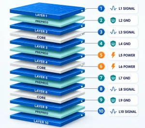
Common PCB Stackup Configurations
PCB board stickup comes in different layers based on the requirement. Common types include 2, 4, 8, and 16 layers. Each layer is essential and plays a significant role in improving performance. A 2-layer PCB stackup is made of two top and bottom copper layers with a separated core. A 4-layer PCB stackup, or multilayer PCB stackup, adds more signal layers with ground and inner power layers.
Flex and Rigid-Flex PCB Stackup Designs
Flex PCBs use a polyimide substance instead of FR-4, which can be bent. Rigid-flex PCBs combine both FR-4 and flexible polyimide in 1 stack. Both eliminate wiring congestion and fit easily into curved spaces. For this reason, you can find it in medical devices and aerospace, as well as dynamic wearable devices.
Metal Core and Metal-backed PCB Stackups
Metal core PCBs use pure metal as their base section for PCB stackup. These metals can be copper or aluminum and are generally attached with thin dielectric or copper foil. A metal-backed PCB connects a normal PCB to a metal plate. Both are designed to transfer heat from power electronics effectively.
PCB Stackup with Sub-lamination
PCB stackup with sub-lamination means building a PCB step by step. In this process, manufacturers first create some layers and press them together, called sub-stackup. Then they add more layers and press them together again to form a complete PCB. This sub-lamination process is usually ideal for complex, high-layer-count PCBs. It reduces drill aspect ratio and improves signal connections.
HDI PCB Stackup Designs
HDI stands for High Density Interconnect. These PCBs use tighter traces, vias, and thinner layers. This improves routing density in a smaller area. Each layer connects through microvias and follows a sequential process to build HDI PCBs. These HDI PCBs are suitable for smartphones, processors, tablets, and other high-performance applications.
PTFE PCB Stackup Designs
The PTFE stackup process uses polytetrafluoroethylene dielectric materials, which have a low dielectric constant and low signal loss. PTFE PCBs use FR-4 materials and often use adhesive materials in layers. People mostly use these PCBs for antenna and radar systems for rapid signal transmission.
Less Common Stackup Designs
Some PCBs may use uncommon designs for special-purpose applications. For example, hybrid stackups that mix FR-4 with ceramic layers or PTFE. Asymmetrical layouts for different mechanical needs are another example. You may also use embedded elements in PCB layers. Each design serves a specific purpose and solves particular problems.
How to Design a Perfect PCB Stackup?
The first thing that matters the most is how complex your circuit connections are. Does it involve so many components together? Or does it involve simple power amplification? Do you need computing, which requires multiple types of chips and different voltage requirements for each component? Organize what you want to do on your PCB and then determine the type of output.\
Choose the Right Material
Choosing the right material depends on your requirements. Select dielectric materials according to your signal and thermal needs. FR-4 materials are perfect for low-frequency use. For high-speed signal transmission, use PTFE or Rogers material.
Estimate the Layer Count
Determine the layer count based on power rails, signal density, and pin count. As mentioned earlier, add power planes and ground to minimize noise and EMI. Place the cores and prepregs symmetrically.
Arrange the Layers
Place the ground and power planes next to the signal layers. It provides a clean return path for signals. Insert high-speed signals near the reference plane. Without using a plane, do not stack two signal lines together.
Lamination Cycles
Lamination cycles are required for high-density stackup PCBs. Using sequential lamination creates bonding between sublayers. Each cycle adds extra cost to the budget. Each cycle also adds heat and pressure. Typically, simple boards take only one cycle.
Ready to Build Yours?
Ready to build your first PCB or turn your PCB design into a finished product? UETPCB provides complete PCB fabrication and assembly services. From wire harness to box building, UETPCB provides complete electronics services. Our team can help you with prototyping and production. Contact UETPCB today to discuss your requirements and start your next PCB project.