
An Austrian engineer created the first PCB in 1943. Since then, many new technologies have appeared in the electronics industry. Among them, SMD, or surface-mount devices, is a core technology. Today, many people want to know in detail about the “SMD Meaning” and its uses.
Electronic devices are getting smaller. As a result, the need for smaller PCBs has increased. Without this, modern devices like your phone or computer couldn’t be so small. SMT technology, which uses SMD, made that possible.
Unlike traditional THT circuits, SMD components mount directly onto the PCB. No holes are needed; instead, tiny pads connect the different terminals of an SMD. This approach lets us fit more components in a smaller area.
What Does SMD Mean? What Does SMD Stand for?
The full form of SMD, or the meaning of SMD, is Surface Mount Device. SMDs come in various types, including resistors, capacitors, inductors, and more. They are small electronic components used on PCBs. Traces connect them, allowing them to communicate and perform different functions.
Engineers place them directly onto the board and solder them to flat metal pads. Unlike traditional methods, they don’t require holes. This method is known as SMT, or Surface-Mount Technology. It replaces older methods like THT in modern PCB manufacturing.
So, SMD means surface-mount device, while SMT means surface-mount technology. The process of assembling SMD is called SMT.
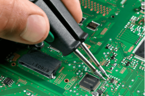
SMD Definition & Core Meaning of SMD
The SMD definition is more than a PCB component type. SMDs are small components that have solder pads instead of pins. This lets you fit more components in a small area. It helps you keep the PCB small while maintaining smooth electrical performance.
SMD stands for a component type based on design and assembly. SMD is not the name of one component. It refers to several electronic components. They have several electrical qualities and functions.
So SMD may signify a few things. It might be a basic passive element or a sophisticated semiconductor package. The type determines terminal size, shape, and number. Even components with the same quality may vary in size or attributes. You can modify a component’s quality by maintaining its Q-factor. High-Q components generally give better signals.
Understanding SMD Package Sizes
SMD package size typically refers to the physical size of the SMD. It tells you how much space the components occupy on the PCB. Two size systems are commonly used: imperial and metric.
- Imperial: Imperial codes are used in standard electronics, and they show length and width. It’s a four-digit code. The first two digits indicate the PCB length, and the last two indicate the PCB width. For instance, a 0603 package means 0.06 inches by 0.03 inches. Common sizes include 0402, 0603, 0805, and 1206. They are quite popular in the USA.
- Metric: Metric codes are also similar to imperial codes. They are also four-digit codes, but they vary by unit. They measure in millimeters. The first two digits show length, and the last two digits show width. For example, a 1608 metric code means 1.6 mm by 0.8 mm. Generally, Europe and Asia use these code systems. So always check before ordering.
Common SMD Package Sizes & Dimensions
SMD packages are commonly identified using imperial and GB size. Both measuring systems typically refer to the same physical package. However, they use different numbering methods. The imperial code is usually based on inches. On the other hand, the Metric code is based on millimeters.
| Imperial | Metric | Size (mm) | Power (R) |
| 01005 | 0402M | 04. x 0.2 | 0.031W |
| 0201 | 0603M | 0.6×0.3 | 0.05W |
| 0402 | 1005M | 1.0 x 0.5 | 0.63W |
| 0603 | 1608M | 1.6 x 0.8 | 0.1W |
| 0805 | 2012M | 2.0 x 1.25 | 0.125W |
| 1206 | 3216M | 3.2 x 1.6 | 0.25W |
Which Package Size Should You Choose?
You might be wondering how to choose the right SMD package size for your project. It typically depends on your board space, assembly method, and project needs. Smaller packages are great for smaller boards. Larger packages, on the other hand, are easier to solder and check.
- 0402 package is ideal for high-density PCB designs. However, it is not suitable for prototyping because it is extremely small.
- 0603 is a good choice when you need a compact design. This SMD package may be suitable for prototyping.
- 0805 typically offers a good balance between small size and ease of handling. It is a practical choice for automated assembly.
- 1206, on the other hand, is comparatively larger. As a result, it is easier to see and handle. It is highly suitable for prototypes, development boards, and circuits.
Various SMD Packages and Their Sizes
As mentioned, different SMDs are available in many package sizes and shapes. The package size may be affected by pins, board space, or overall component size. The table below typically shows some common SMD packages and their sizes.
| Package | Pins | Body Size (mm) | Pakage | Pins | Body Size (mm) |
| SOT-23 | 3 | 2.9 x 1.3 x 1.0 | SOT-23-5 | 5 | 2.9 x 1.6 x 1.0 |
| SOT-89 | 3 | 4.5 x 2.5 x 1.5 | SOT-223 | 4 | 6.7 x 3.6 x 1.8 |
| SOT-252(DPAK) | 3 | 9.9 x 6.5 x 2.3 | SOT-263(D2PAK) | 7 | 10.3 x 8.1 x 2.3 |
| SOD-123 | 2 | 2.8 x 1.8 x 1.0 | SOD-323 | 2 | 1.7 x 1.25 x 0.95 |
| SMA (DO-214AC) | 2 | 4.4 x 2.7 x 2.1 | SMB (DO-214AA) | 2 | 5.0 x 3.6 x 2.2 |
| SMC (DO-214AB) | 2 | 7.9 x 5.9 x 2.4 | SOIC-8 | 8 | 3.9 (body width) |
| SOIC-14/16 | 14-16 | 3.9 (body width) | TSSOP-8 | 8 | 3.0 (body width) |
| SSOP-16 | 16 | 5.3 (body width) | MSOP-8 | 8 | 3.0 (body width) |
| LQFP-32 | 32 | 7 x 7 | LQFP-48 | 48 | 7 x 7 |
| LQFP-64 | 64 | 10 x 10 | LQFP-100 | 100 | 14 x 14 |
| LQFP-144 | 144 | 20 x 20 | QFN-8 | 8 | 2 x 2 |
| QFN-16 | 16 | 3 x 3 | QFN-32 | 32 | 5 x 5 |
| QFN-48 | 48 | 6 x 6 | QFN-64 | 64 | 8 x 8 |
Common Types of SMD Components
SMD components come in many types, sizes, and properties. Each of them serves a different purpose in the same electronic circuit. Some SMDs control current, while others may store energy or switch signals. Some (chips) may process information. To understand SMDs, it’s also crucial to understand how each one works.
| Component Name | Typical Application | Types |
| SMD Resistors | Current limiting, voltage division, and signal control | Thick-film, thin-film, metal-film, and wire-wound |
| SMD Capacitors | Filtering, energy storage, and noise suppression | Ceramic, tantalum, aluminum electrolytic, and film |
| SMD Inductors | Filtering, energy storage, and RF circuits | Wire-wound, multilayer, ferrite, and power inductors |
| SMD Diodes | Rectification, voltage protection, and signal switching | Schottky, Zener, TVS, switching, and LED |
| SMD Transistors | Switching, amplification, and signal control | BJT, MOSFET, JFET, and IGBT |
| SMD ICs | Processing, control, memory, and signal management | Microcontrollers, processors, memory ICs, amplifiers, and logic ICs |
| Other SMD Components | Circuit protection, timing, sensing, and connection | Fuses, crystals, LEDs, sensors, thermistors, and connectors |
How Are SMD Components Mounted on a PCB?
Understanding the SMD Meaning also includes how SMDs are mounted on a PCB. As the name implies, these components are mounted directly on the surface of the PCB. No holes need to be drilled. You need two or more pads for the SMD to mount on.
Manual SMD Mounting
Manual SMD mounting is tricky and requires a professional hand. In general, automated mounting is used for SMD mounting. However, if you are making prototypes or repairing PCBs, then the manual method is feasible.
First, apply solder paste or flux to the corresponding pads on the PCB. Add the appropriate amount of solder. Then place the SMD in the correct position. Then use a hot air gun or thermal gun to melt the solder. Once the solder is melted, the SMD will automatically be in position.
Some experts do it a little differently. They first put the SMD on the pad. Then they use a soldering iron to melt the solder and attach the SMD to the PCB. The right method depends on the SMD size and the operator’s expertise.
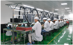
Automated SMD Mounting
When in mass production, manual SMD mounting is time-consuming. Therefore, an automated SMD mounting method is preferred.
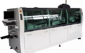
A pick-and-place machine picks components from the reels, trays, or other feeders. Then it places them onto the correct positions on the PCB. Before this step, solder paste is normally applied to the respective pads. The board then passes through a reflow oven. The heat melts the solder paste and permanently attaches the components to the PCB.
Final Thoughts
Electronics are made differently today because of SMD parts. They are better in many ways than older methods. Most SMD parts are smaller, so you can fit more of them on a board. SMD also allows automated assembly, which is another plus. Because of these three benefits, SMD is a big part of the electronics industry today.
However, SMDs also have limitations you should know. Very small packages can be difficult to handle, check, and repair. Some packages also need careful PCB layout and a proper soldering process. To reduce these problems, you may need to select components carefully. You might even need to redesign the PCB layout and change soldering methods.
Therefore, choosing an SMD is not only about finding the smallest package. You must consider various factors. This article has covered the SMD Meaning, its types, applications, advantages, and limitations. We hope you now have enough information about this technology. For more information, feel free to contact us.