PCBs are the brains of every electronics. It is usually small and flat-shaped. Although there are some large circuit boards, most of them are tiny. Now, when manufacturing these PCBs one by one might take a lot of time. Because of this, you can get less productivity and high labor costs. How do we solve this problem? That’s where PCB panelization comes in handy.
Depanelization is another essential topic to discuss. It mostly involves separating each PCB from a penal. Assume you’re working on a complex project. Each PCB in your project must be accurate and fit exactly to the device. In this case, if the depanelization is done in the wrong way, you might not get the expected result. Therefore, following the right destabilization technique is very important.
This article will cover all the ins and outs of PCB panelization and depanelization. It will mainly highlight the different methods of panelization and depanelization. From v-scoring to laser cutting, there is a lot to cover.
What is PCB penalization?
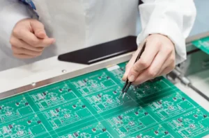
PCB panelization is the process of grouping multiple PCBs onto a single larger board. This strategy allows you to make various PCBs at a time. You can either create a set of PCBs for a device or multiple PCBs of the same design. As a result, you can save both time and money.
In electronics, efficiency is everything. Panelization, in this case, plays a crucial role by reducing handling and maximizing material use. Instead of working with one tiny board at a time, you can handle an entire panel. After the components are mounted, you can safely separate them.
There are plenty of situations where panelization makes sense. For example, when boards are too small to be efficiently produced one at a time. It’s also helpful when you have several different boards that need to be assembled. You can combine them on one panel and save time in the production line.
Why is PCB Panelization important?
You already know that PCB panels typically come with multiple PCBs. Making a PCB panel generally allows you to work with many boards at once instead of one piece. But why is it so important? There are several reasons why PCB Panelization is important in electronics. However, the following four points are the most noticeable.
Fast Production
PCB panelization speeds up the entire production process. Imagine trying to handle one PCB at a time. It would definitely be slow. But with panelization, you can process several boards all at once. On single panels, the more boards you work on, the more downtime you can reduce when switching between PCBs. The number of boards generally depends on the size.
This strategy can drastically reduce production time. Fast production is key, especially when there is high customer demand.
Less Cost Per Part
PCB panelization also lowers the cost per part. By reducing downtime by using PCB panels, you can produce more parts in less time. Besides, when you work with a single PCB, you may need more equipment. As a result, it increases the manufacturing expenses.
With PCB panelization, fewer machines and, eventually, fewer people will be needed to operate. This typically reduces the final product’s cost significantly.
Ensures Safety
During PCB fabrication, the boards undergo many stages. In each stage, robot hands or human hands place the components on the PCBs. As you can see, the boards go through multiple handling processes. This not only increases the wear and tear but also compromises the safety of the PCB.
PCB panels generally have a protective boundary. This boundary protects the smaller PCB inside the panel, making the whole panel less likely to be damaged than a single PCB. When dealing with fragile components, you must ensure safety during the production process. It reduces the risk of breakage and saves both time and money on repairs.
Easier Handling
PCB panels are easy to handle and much simpler to process than individual tiny boards. For individual PCBs, you must focus on safety during production. This typically requires extra special equipment, making the production process much more complex. In this case, PCB panels do not need extra safety equipment; therefore, they are easy to process.
PCB panels are also easy to move from one location to another. They keep everything neat, allowing you and the product machine to work on them smoothly.
What is the Depanelization Method?
You are already familiar with PCB panelization. However, it is equally important to know about depanelization.
Depanelization is the process of disconnecting all the PCBs from the panel. As you know from the previous section, a large panel consists of several small PCBs. Depanelization is nothing but removing those PCBs from the panel. This is a very important stage throughout the overall formation of printed circuit boards.
During the making of the panels, the PCBs are made in such a way that you can easily remove them without harming them. Yet, there are professional techniques that are followed during depanelization. Before explaining the two major types of deionization techniques, let’s check why this process must be perfect.
(1) Improper depanelization can damage sensitive components.
(2) Manual handling or incorrect methods can create rough edges on your PCB. This might interfere with the assembly of the final product. It becomes critical when it comes to precision components.
(3) Using the right method also speed up the production process.
(4) The right technique also minimizes the errors.
(5) Using the right method gives constant results all the time.
Method #1 V-Scoring
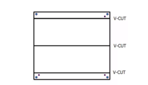
V-scoring is one of the most common methods used in PCB factories. As the name suggests, this method creates a V-shaped groove along the PCB’s edges. The remaining part of the groove is generally strong enough to hold the main board. After putting the components in the right position, you can smoothly remove the PCB by simply cutting or snapping it off.
There are some benefits of the v-scoring depanelization method over PCB tab routing. First, it is very simple. Second, v-scoring is perfect for panels with flat, straight edges that define basic patterns of panel arrangement. Third, v-scoring is faster than PCB tab routing. Finally, it is a very cost-effective method.
Although this method offers many pros, it still has some cons. These cons typically make V-scoring less common in PCB factories. First, you can not use this method for complex designs with no straight edges. Second, while snapping the PCBs, the impact may be distributed to the PCB and may harm the components.
Method #2 Tab Routing PCB
Tab routing is much more different than v-scoring. Although both methods aim for the same purpose, their construction is quite different.
As the name suggests, PCB tab routing generally has several little tabs around the PCB’s edges. Once the PCB panel is fabricated, you can simply separate it by snapping it off. However, if these tabs have pores, they may create rough edges.
PCB tab routing is especially suitable for complex PCB designs. This method can adapt different board layouts and designs. You can create the tab in different ways. However, perforated tabs are generally more effective because they distribute stress evenly. Because of this, you can reduce the risk of damage.
PCB tab routing also has some limitations. First, it needs extra material or tab routing. Besides, improper tab removal may damage the PCB edges. Finally, and most importantly, it is not suitable for thin boards.
How Does Depanelization Work?
Whether you are following v-scoring or PCB tab routing, you should follow the proper technique of removing the PCB. This depanelization work may differ based on the size and complexity of the PCB. However, mostly the following techniques are followed:
Manual Depanelization
This approach is the simplest one. Although it is the easiest and simplest way by hand, it is risky. When doing it, you must be careful so that you don’t damage the PCB. Although this method is recommended, you could use it for low-volume production.
Punch or Die Cutting
This method is faster. Punch or die cutting involves applying pressure to the boards and cutting them out with a machine. Although it is rapid and precise, the setup might be costly. Once set, however, it is ideal for high-volume jobs.
Saw Cutting
Saw cutting uses a tiny, revolving blade to cut through the PCB panel. This approach is precise and clean, but it can be slower than punch or die cutting. Saw cutting produces dust, which can harm the boards if not regulated.
Depaneling Router
A depaneling router uses a spindle to carve out each PCB. It’s like a tiny wood router but for circuit boards. This method provides great precision, but it’s not the fastest. Routers are good when the boards have complex shapes that other methods can’t handle.
Laser Cutting
Laser cutting cuts through the PCB with a powerful beam. This method is totally non-contact and technically lowers the chances of injury. It is extremely precise and can handle intricate designs. However, it is more expensive and slower than some of the other options.
Summary
PCB panelization means grouping several PCBs onto a single panel. On the other hand, depanelization means removing the PCBs from the panel. Indeed, panelization is an efficient and quick approach to making hundreds of thousands of PCBs. However, the processes of penalization and depanelization are different based on different types of PCBs.
You must also be aware that a good PCB panel design is critical for high-quality PCBs. The optimal design reduces waste costs and boosts your production. Obviously, poor design can result in problems, delays, or even failure. If you need more help with PCB panelization guidelines, contact us.


