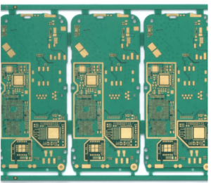
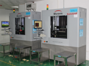
We can see the magic of electronic devices in almost every sphere of our lives. But have you ever wondered what creates that magic? Inside the classy-looking gadgets, the components are pretty sophisticated. Altogether, they make up “Printed Circuit Board (PCB).” Hence, precise industrial PCB production is vital for electronics. UETPCB does the job of PCB production with utmost care and due sincerity. Besides PCB manufacturing, they also provide all-out solutions for your PCB.
Now, the question is, what does a PCB do? In simple words, PCB enacts human commands by guiding electronic signals. Each component of a PCB has a specific function for the device. As a result, every step of PCB manufacturing is crucial. From this article, you can expect to learn how to make a printed circuit board. Let’s explore PCB manufacturing techniques right from its initial design to assembly.
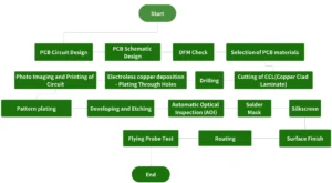
PCB Manufacturing Process: Step-By-Step
PCB manufacturing is the outcome of some technical activities. It needs both proper planning and supervision. Manufacturing printed circuits is a lengthy and complex operation. A PCB factory like UETPCB is ready to accept the challenges of these complexities. Circuit board manufacturing starts with designing it and preparing the file. The manufacturing ends with profiling and V-scoring.
PCB Designing And File Preparation
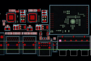
First, the process begins with preparing the design of the components on the board. This design allows you to visualize the electrical connections within the electrical components. Then, you can choose the components and define how to interconnect them.
After that, you can convert your design into a physical layout. Software like EasyEDA can help you with this. The layout is essential to display the position of the components on the board. In this case, you should be aware of the factors like power distribution and manufacturability.
Then, you can verify the design with the desired specifications. Is the trace width or spacing appropriately assigned for the layout? Any error in the verification may lead to board failure.
After preparing the layout, another conversion into industry-standard file formats is needed. You can use Gerber files to depict the graphical data of a PCB. NC drill files regulate all the information for the hole drilling operations in the PCB. Assembly drawings and BOM tell us about component placement and assembly identification.
You now have to send these files to a PCB manufacturer. Only these files can make accurate circuit board manufacturing possible.
Film Generation For Imaging
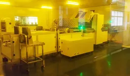
Film generation is vital to the photolithographic process of PCB manufacturing. A photoplotter generates high-resolution films with precise patterning. The film component is a light-sensitive material. Films can be either positive or negative. The design area is apparent in a positive film. However, in a negative film, the design area is opaque, and the rest is transparent.
Film resolution is vital for the accuracy of the circuit traces. High resolution means the copper traces must be finer and more detailed. It is crucial for high-density PCBs. A film comes with a photosensitive layer on the circuit board.
During photolithography, the film remains over the printed circuit board. The photosensitive material reacts in the presence of UV light through the film. In this way, you can get the required pattern on the board. The developed and marked pattern creates the conductive paths. You can expect accurate and high-quality PCBs from quality films. It is also linked to the precision of the entire PCB manufacturing.
Printing Copper Patterns
Printing copper patterns is at the heart of circuit board manufacturing. It’s nothing but transferring the circuit design onto the PCB substrate. The conductive routes of the electrical components on the board follow the patterns. Screen printing, inkjet printing, or photolithography are suitable for this purpose. A thin layer of copper wraps up the PCB substrate.
An insulating material like FR4 is often the main ingredient of the substrate. It’s a flame-resistant fiberglass. The introduction of the photoresist to the copper-coated board protects certain areas. These areas should remain intact while the exposed copper needs to be etched away. The photomask is sensitive to UV light.
So, the aligned photomask over the PCB hardens the photoresist in UV light in certain areas. It applies only to areas not blocked by the film pattern. This way, the copper circuit design passes onto the photoresist layer. The exposed PCB is then treated to reveal the remaining copper pattern.
Etching Unwanted Copper
After transferring the copper pattern, the unwanted copper remains in a circuit board. This step cleanses the unwanted copper. Etching identifies the conductive channel and separates traces. Using a chemical solution is a great way to do this. Hydrochloric acid and hydrogen peroxide are typically used in this case. The board remains harmless in the solution. But the unwanted copper dissolves in chemicals. That leaves behind the desired circuit pattern.
The PCB factory can’t compromise on protective measures to handle the chemicals. You must wear safety gear during chemical etching, cleaning, or whatever you say. The place where you are doing this must have a good airflow.
Aligning Different Layers And Examining Them
Once the unwanted copper has been removed, verifying the layers is time-consuming. In general, this stage of the production process checks whether the circuit is arranged correctly. Why is this check so important? This check is necessary to ensure there are no circuit problems. The proper functioning of any circuit is subject to this inspection.
The different parts of a PCB or circuit must be assembled correctly. Optical alignment or automated optical inspection (AOI) systems provide that precision.
After alignment, the layers are checked in a fully controlled testing lab, which generally guarantees the PCB’s safety. Here are three things you must be careful of. First, look at the connections. Do you see overlapping? Second, did you find any layer slightly shifted to any side? Third, check other dissimilarities as well. Note that these problems might cause electrical failures. Because of this, experts always use optical tools to check them.
Layer Stacking And Bonding
Great! We can move to our next step. Your layers are stacked perfectly, and you have checked them right. Now it’s the turn to combine them. This step is unavoidable for creating strong, functional, and multi-layer PCBs.
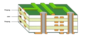
The prepared copper and insulation layers have to be in the correct order. A crucial material used here is prepreg to stack up the layer. In other words, it is called pre-impregnated resin sheets. Applying this material gives excellent insulation and bonding to the layers. Prepreg is nothing but semi-cured resin. It becomes cured upon applying heat and pressure during bonding.
To combine the layers stacking up together, use the lamination method. You need to use enough heat and pressure during this step. Later, a computerized system melts and hardens the prepreg material. Because of this, the PCB layers can adjoin in their respective secure places.
Drilling Holes
The next step is to drill the circuit board. You can create the holes using mechanical and electrochemical tools. Among the mechanical methods, you can choose punching or laser cutting. On the other hand, chemical milling is the best electrochemical technique.
Indeed, drilling must need accuracy. An X-ray locator determines the precise locations to drill to guarantee correct positioning. A buffer under the drill target avoids hole deformation and contamination of edges.
There are no people here. A computer controls the drilling process and locates the position of each hole according to the design file. Each hole needs some meticulous detail. After drilling on the panel, a profiling tool trims excess copper along the panel’s edges.
Copper Plating Deposition
Before copper plating, the PCBs must be cleaned. You can use distilled water in this case. After this, they get ready to adhere to the proper copper. Chemical etching cleans up the surface, and slight roughening makes it perfect. The PCB works as a cathode and connects to a power supply, so electrochemical deposition occurs. In industrial PCB production, you may call it a copper bath.
Copper forms a uniform layer if you take care of three things. You must be careful to control the current density, temperature, and, lastly, the composition of the bath properly. Of course, it is necessary to develop sound connections to ensure long-term uses. But, the thickness of the plating varies depending on the design of the PCB.
Imaging The Outer Layer
You need to repeat some processes from the third step in this step. The difference is that this time, you target only the outer layer of the PCB.
The process takes place in a yellow room. UV light can affect the photoresist, but yellow light neutralizes that effect. After developing and checking, the outer layers undergo plating as the inner layers. In this case, tin plating remains an extra protective layer.
Electroplating For Conductivity
Electroplating is the process of creating layers of metals. Copper or gold are excellent conductors of electricity, so you can use them for a PCB. But before you do this, you must rewash the PCB. Then, put it in the electrolytic solution for the bath. With electricity, salt, and electrolytes, your PCB gets the electroplating.
An electric current through the bath deposits metal ions on the exposed copper. This process also coats the inner walls for multilayered PCBs. Electroplating makes the PCB more viable. It makes the board fit against electrical and thermal stress.
Final Copper Etching
This step is the final copper etching process. As usual, it removes extra copper from the PCB. This etching process is generally done in an etching solution. In most cases, ferric chloride or ammonium persulfate is used. It typically takes care of unprotected copper areas.
This step emphasizes that the photoresist should only let the selective copper traces. After the completion of the etching, the remaining photoresist should vanish. That leaves clean, well-defined circuit paths.
Applying The Solder Mask
The solder mask is more of a security layer. Its application to the PCB prevents unwanted areas from being touched during assembly. This layer is active against short circuits and guards the copper traces from degradation. The solder mask is usually a green, liquid, or dry film.
The mask spreads all over the board. It is then exposed to light through a mask to define where it should stay and where it should not. The final destination of the mask is baking to harden it and make it durable.
Surface Finishing
Once everything is done, your PCB will undergo the surface finishing process. This step is necessary because it prevents copper from oxidizing and improves soldering capability. You could use various methods, such as HASL, ENIG, or OSP.
Each method adds a thin protective layer to the copper surface. Whatever the process, it permits easy soldering. The choice primarily depends on your design needs.
Adding The Silkscreen
We are entering the last few steps. The silkscreen is a printed layer on the PCB. It labels, symbols, and markers. It shows the directives of component placements and guides assembly. The ink is white or contrasting colors over the solder mask.
Electrical Testing And Certification
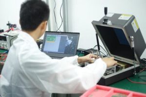
A continuity test certifies the absence of any broken connection. Flying probe testing does more complex checks. Other testing methods may be needed for your case. Once tested, your PCB is ready for use.
Profiling and V-scoring
Finally, one thing remains: shaping the PCB. Profiling and V-scoring are two of the most popular methods for separating PCBs.
In this case, profiling typically uses routers or lasers to create the outlines. Then, V-scoring notches are made along the breaks in the copper tracks on the board. To learn more about this step, read our article “What is PCB Panelization?”
Why Would You Choose UETPCB As Your Trusted PCB Manufacturer?
PCBs are the heart of every electronics. Any tiny error can lead to system malfunction. So, PCB manufacturing must be handled with care and through continuous monitoring. In this case, a PCB factory must have years of experience to earn your trust and confidence.
UETPCB is an international player in the industrial PCB production arena. We track every single step of PCB manufacturing to produce high-quality PCBs. We provide one-stop solutions to your PCB-related problems to keep you tense-free. Our PCB manufacturing techniques are unique from any other producer. You can always have the best choice here.


