PCB assembly involves putting the electronic components on the PCB board, also known as PCBA. There are different PCB assembly processes, and BGA assembly is among the most popular.
In the modern world, people seek advanced PCB assembly processes. As you know, electronic components are getting smaller and becoming more convenient. Thus, the demand for high-density PCBs is sky-high. These PCBs offer faster operation and better thermal management. The BGA assembly process allows you to make such PCBs.
In this article, you will learn more about Ball Grid Array assembly. You will mainly learn what this PCBA is and what their types are. Later, you will also be familiar with various BGA assembly testing processes. Finally, we hope you will get sufficient knowledge about this technology.

What is the Ball Grid Array Assembly?
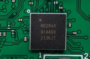
BGA means ball grid array. From the name, you can guess that this assembly process is done using some types of balls in a grid array. BGA assembly is a PCBA process used to attach BGA components to PCB. BGA components are also known as BGA packages.
To understand BGA packages, it is also essential to comprehend PGA packages. PGA stands for Pin Grid Assembly. PGA packages use an array of pins to be connected to the PCB, making them ideal for easy socket mounting. BGA packages are more advanced than PGA packages. The main difference between BGA and PGA packages is the connection method. One uses protruding pins, while the other uses solder balls.
BGA Assembly Process
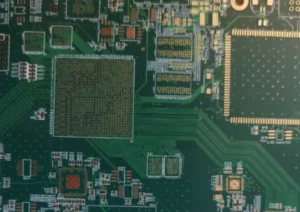
The BGA Assembly Process typically involves three significant steps. The first step is to design the PCB for BGA, which must perfectly accommodate BGA packages. They need sufficient space for solder balls and traces. In addition, you must also pay attention to proper pad sizes and solder mask openings. Also, it is crucial to place the Vias to avoid interference with the solder joints.
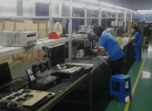
The second step is to place the BGA Packages on the PCB. You can use a pick-and-place machine to ensure the BGA package is aligned and placed accurately on the PCB. Accurate placement is critical to ensure all solder balls align with the PCB pads.
The third and most crucial step is the solder reflow process and joint formation. You must heat the PCB and BGA in a reflow oven. The heat inside the oven melts the solder balls and creates connections between the BGA and the PCB. You must control this heating and cooling process. Appropriate heating and cooling ensure strong and reliable joints.
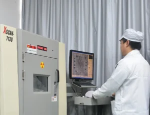
Later, you can test the assembled PCB under an X-ray inspection device. This will ensure that the solder joints have been perfected and connected to the PCB.

Benefits of BGA Assembly
BGA packages are the advanced PCB components that came after PGA components. Some limitations of PGA components create the demands for BGA parts. PGA components have limited pin density.
The spacing between the pins typically limited the number of connections. PGA packages are much larger, eventually making electronic devices bigger. PGA components offer poor thermal management, which reduces their efficiency.
All these significant limitations of PGA components make BGA components popular in the PCB industry.
(1) A ball grid array usually makes BGA components much smaller. Thus, you can create more compact designs.
(2) Ball Grid Assembly offers better thermal and electrical properties. It can dissipate temperature more efficiently due to its design. As you know, shorter connections improve the electrical performance. Therefore, BGA PCB assembly offers much faster and more reliable devices.
(4) BGA packages can handle a larger number of pins so that you can make more connections in a small area. This is perfect for high-frequency applications. Implementing BGA assembly allows you to design more advanced systems without increasing the PCB size.
(5) The shorter connection paths in BGA assembly reduce signal interference. As a result, you can expect high-quality signals and stable communications.
(6) The BGA assembly is strong and reliable. The solder balls offer robust mechanical connections, which makes them ideal for vibration and stress applications.
Limitations of BGA PCB Assembly
BGA assembly has many advantages, but it also comes with some limitations. These challenges are essential to consider when using BGA electronic manufacturing.
(1) Testing BGA solder joints is tricky. The connections are under the chip and not visible. You can not use traditional methods to detect issues. You will use advanced tools, like X-ray machines, to test the BGA assembly PCB.
(2) Reworking with BGA PCB assembly is not easy. You will need special tools to remove and replace BGA components. Also, professional hands are needed to re-install the packages on the PCB.
(4) BGA assembly is much more expensive than PGA assembly. Its better thermal management, compact design, and durability make it more popular. However, manufacturing BGA components is also complex and advanced, so the cost of BGA assembly is also very high.
Types of BGA Package
BGA packages, or Ball Grid Array Components, come in various types. Each type is specially designed for a particular application or project.
Plastic BGA (PBGA)
Plastic BGA packages are incredibly lightweight and cheap. People prefer using PBGA on computers and smartphones PCB. Compared to other types, these BGAs offer good thermal and electrical performance.
Ceramic BGA (CBGA)
Ceramic BGA packages are better choices because they last longer and work better. Indeed, ceramic is great against high temperatures. They can withstand harsh conditions. BGA packages are used in the automobile, aircraft, and industrial fields.
Tape BGA (TBGA)
Tape BGA packages are made from bendable tape and are great for applications that require speed and regularity. They are also great for high-tech communication devices.
Micro BGA Package (µBGA)
As the name suggests, these BGA packages are much smaller than other types. Micro BGA packages are capable of doing high-frequency work. They are perfect for portable devices. Digital watches, microbots, and nanotechnology all rely on this micro BGA.
Fine Pitch BGA (FBGA)
These BGA packages usually come with more solder balls than the regular ones. This means that FBGA chips can do more at the same time. These BGA packages are prevalent for processing devices like CPUs. FBGA makes sure that electricity connections work better.
Cavity Down PBGA
Cavity Down PBGA has a recessed cavity for improved head dissipation. If your project needs better thermal management systems, try these BGA packages.
High Thermal BGA
High Thermal BGA packages are prevalent for power-intensive applications. They are specially designed to handle high heat loads.
Flip Chip BGA (FCBGA)
The Flip-Chip BGA links directly to the base, improving electrical performance. Many computers and high-speed chips use it.
Testing for BGA Assembly
Testing is an important part of putting together a BGA. Why testing is so necessary? This way, you can guarantee a good quality product. Also, you can take the necessary steps to deal with defects. BGA packages are tested in several different ways. The method used is mainly determined by the stage of output and the needs at hand.
Electrical Testing
Electrical testing is the most basic method used in factories and repair stations. Like other testing methods, it checks the functionality of the BGA assembly. However, it mainly checks continuity to determine whether there are short circuits or broken connections. In factories, digital test probes or fixtures measure electrical signals.
Electrical testing is fast and effective. However, it may not detect physical defects like solder joint voids.
Optical Testing
Optical testing means testing by optical devices. This testing mainly inspects the surface of the BGA assembly. It helps you detect various visual defects. Typical examples are misaligned components or damaged balls.
In this case, two types of optical testing devices are used. The first one is the MVI, or manual visual inspection. This method typically uses magnifiers to check assemblies. The other one is AOI or automated optical inspection. This method uses high-resolution cameras. You can zoom in and check every part of the PCB.
X-ray Inspection
X-ray machines help you detect defects that you can not do with other testing methods. This testing method identifies hidden defects in BGA assemblies. It offers you with a detailed view of solder joints beneath the package.
There are four main types of X-ray tests. A 2D X-ray makes a flat picture of the part, which is excellent for basic analysis. A 3D X-ray, on the other hand, allows you to see advanced flaws in great depth. Void detection finds places where solder joints have air holes. The final one is alignment analysis, which checks whether you have included the components correctly.

UETPCB BGA Technology
UETPCB is a leading PCB manufacturer. BGA assembly is one of its popular and most demanding services. The company offers high-quality solutions for compact, high-performance electronic devices.
UETPCB uses advanced equipment and quality control measures. The BGA assembly performed in this facility always ensures accurate connections. UETPCB guarantees improved electrical performance. Your device gets reliable solder joints and optimal thermal management.
The company offers various BGA options, including PBGA, CBGA, and FCBGA. You can customize these options according to your project needs. The company also supports custom designs for unique applications.
Please contact us if you have any questions or are interested in PCB assembly processes. We have a very professional team of experts who are always happy to assist you. You can also navigate to our services pages to learn more about what we do.

