
Custom PCB
What Is Custom PCB?
A custom PCB is designed and manufactured for a unique electronic device or project. Customers who did not find a suitable PCB from our stock can choose this option. Alternatively, you can employ specific techniques during PCB design. It may enhance flexibility and alignment with your fabrication and assembly requirements. This approach of making PCBs is more cost-effective than fully customized options.
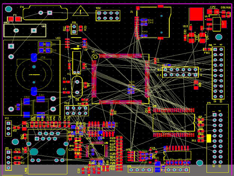
Whether you desire full-custom PCBs or intend to create custom PCBs, you must have some basic PCB understanding. Firstly, you should know the process of PCB fabrication and assembly. Next, learn the suitable materials for PCBs, their types, and their characteristics. Finally, other basics include the PCB component, design, layout, and reverse engineering software.
Why You Need Custom PCB Boards?
Custom PCB can be divided into two groups: full custom and design custom.
The full-custom PCB is more flexible and advanced than the design custom PCBs. It is usually used in high-standard industries such as the medical or aerospace industries. These industries require an exceptional design for their devices.
Design custom PCB is cheaper than the full-custom PCB. It is more complex and flexible than the typical type. It doesn’t offer comprehensive custom PCB design but has a more complex structure than the normal. It also provides a unique and professional appearance. Compared with the full-custom PCBs, the design custom boards have a lower cost and fast production circle.
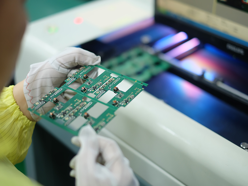
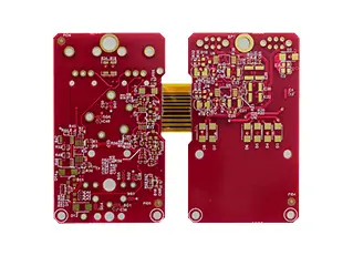
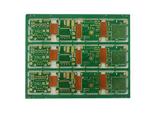
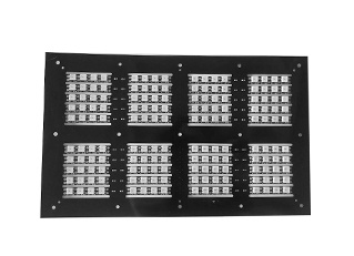
Custom PCB boards come from four methods: PCB fabrication, PCB assembly, PCB coating, and PCB inspection. PCB manufacturers provide specialized coating and inspection services. You can select your unique PCB prototype’s type, material, and production method. On the other hand, PCB production and assembly processes offer flexibility in customization. Custom PCB manufacturers assist in tailoring your PCB to your specific needs.
The following indicates two fundamental processes of PCB fabrication and assembly:
Eight steps of PCB fabrication:
Step 1: Creating a designed layout on the copper-clad laminate
Step 2: PCB manufacturers will etch or remove excess material from inner layers to reveal images and pads.
Step 3: Laminating printed circuit board materials at high temperatures to create the PCB layer stack up.
Step 4: Creating mounting holes, through-hole pins, and vias on the PCB
Step 5: Etch and remove the excess copper of the surface layer to reveal images and pads.
Step 6: Placing plating pin holes and via holes.
Step 7: Creating a protective coating or solder masking on the surface
Step 8: Printing silkscreen, logos, or other markings and installing polarity indicators on the surface.
Five steps of custom PCB board assembly:
Step 1: Adding Solder Paste
Step 2: PCB Printing Pick and Place
Step 3: Soldering
Step 4: Inspection
Step 5: Testing
Material is the second core during the PCB manufacturing process. Custom PCB designers must consider functionality and wear resistance in their designs. These considerations are crucial to ensure the regular operation of custom PCBs. Various electronic products require distinct PCBs to utilize their specific functions efficiently. These factors include dielectric constant, flame retardance, transition temperatures, and mitigated loss factors. They also relate to thermal performance and dimensional stability, among others.
Therefore, some excellent materials are most popular to use as the material of PCB production:
FR4 epoxy laminate and prepreg
This material features good electrical, thermal, and mechanical characteristics. It also provides an excellent strength-to-weight ratio. Therefore, FR4 has become the ideal material for most electronic applications. Besides, this material meets specific NEMA LI 1-1998 standard requirements. In addition, FR4 laminates and prepreg are usually used for the custom printed circuit board. They are prevalent for making with lower layer counts, generally less than 14 layers.
Polyimide laminates and prepreg:
This material is more resistant in harsh and higher-temperature environments. Compared to FR4, this material made custom-printed circuit board materials more expensive. However, they provide improved electrical performance. Moreover, This material is stable during thermal cycling with less expansion property. As a result, they are very suitable for higher layer count constructions.
Teflon laminates and bonding plies:
This material’s excellent electrical properties make it ideal for custom PCB manufacturing. Teflon laminates and bonding plies can provide high-speed capabilities to the designers. As a result, they have become the perfect material for high-speed circuitry applications. Ultimately, it is more expensive than polyimide.
Flexible laminates:
This material is thin and prevalent for the electronic design that needs to fold the PCB. Generally, this material is made from higher-temperature materials such as polyimide. Laminates may also come from low-cost materials such as PEN and polyester.
Other custom PCB production materials include BT, ceramics, and cyanate ester.
We truly understand the latest technologies in custom PCB design and manufacturing. We ensure our customers get the most appropriate solution. Whether it’s fast delivery, reliable, and stable production of the highest technology PCBs, we can help you achieve your goals.
UETPCB is a renowned custom-printed circuit board manufacturer. Choose us as your custom printed circuit board manufacturer for a perfect experience.