
Sometimes, there may be a tolerance of voltage or current in electrical connections. These situations are nothing unusual. They may indeed cause some damage to your circuit. However, one of the best ways to solve this is to use grounding (GND) in electronics.
GND is the short form of grounding. Although it is not directly connected to the physical ground, it is crucial for every circuit. Here, the term ‘earthing’ may confuse you. We often use this term, though, in building wiring.
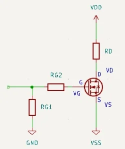
GND usually creates a return path for fault current in the circuit board. This means that if the PCB has any fault current, it can discharge it, which does not affect other components. Most circuit boards rely on GND. However, floating or battery-powered devices can operate without a GND.
GND also ensures the quality of the signal. Let’s take an example. You may have noticed the speaker crackling before. Do you know why this happens? Yes, you are right. It is mainly due to poor grounding.
The ground is generally of many types. The specific type typically depends on its uses. In this article, you will learn about GND and its different types. You will also learn about the importance of grounding and its numerous applications.
Why is Proper Ground Crucial in PCB Design?
The primary purpose of a GND or Grounding is to save the electronic devices from fault currents. However, it is also necessary for signal quality, noise reduction, and voltage stability. You can find different types of grounding based on various uses.
Suppose you design a PCB and do not provide any grounding. What can happen when you flow electricity through it? If you pass the right amount of voltage and current, you may not notice such a problem. However, issues like voltage spikes, ground loops, or floating references can arise anytime. Due to this, noise can occur in your PCB. In this way, your components gradually malfunction before their due time. So, you may not get the proper longevity.
It is essential to note that high-frequency circuits require a low-inductance return path. If this is not maintained, the signal quality can never be maintained. Therefore, it is crucial to use grounded PCBs. In multi-layer PCBs, an entire plane is necessary for grounding.
Proper grounding is one of the major solutions to achieving power stability. Poor grounding can cause ground bouncing. When more than one IC switches quickly, a sudden current surge is created in the ground plane.
Also, if there is inductance and high impedance in the ground path, there will be a voltage drop. For these reasons, instability or power fluctuation can be seen in the signal. Therefore, you must ensure proper grounding.
Common PCB Grounding Techniques in PCB Design
As mentioned earlier, the grounding type can change depending on the need, which can also come from the PCB design requirements. Below are seven types of grounding used in printed circuit boards (PCBs).
#1 Single-point grounding
As you can understand from the name, these groundings end at one point. Each ground trace of the PCB meets at a ground point. You may mainly see them in low-frequency circuits.
#2 multi-point grounding
This type of grounding has more than one ground point. These ground points are created based on different components’ needs or positions. This type of ground (GND) is more common in high-frequency printed circuit boards (PCBs).
#3 Ground Plane
This type of grounding uses an entire plane of the PCB. It is typically a large, dense, and conductive layer. Multi-layer PCBs use this type of grounding.
#4 Star Grounding
The system attaches all ground connections in a star-like pattern. Its main job is to block noise coupling between sub-circuits. This type of grounding is suitable for sensitive analog and audio systems.
#5 Ground Pours
A ground pour is a large area filled with copper. It connects to the ground and guarantees a flow to other components. This type of GND is ideal for heat dissipation and EMI reduction.
#6 Guard Traces
This type of grounding is located next to the signal line. This unique position mainly reduces noise and prevents crosstalk. This grounding type is ideal for devices with high impedance or sensitive signals.
#7 Split Ground Plane
This type of grounding is found in different circuit board sections. The grounding connections are located in isolated states throughout the circuit. It uses separate analog, digital, and power grounding to reduce interference.
Best Practices for PCB Grounding When Designing a PCB
Along with other rules, placing the GND at the right location is also crucial when designing a PCB. Here are some tips that you can consider while planning your PCB.
#1. You can use a solid ground plane if your PCB requires high-performance signal quality. As you know, the solid ground plane is often seen in a multi-layer PCB stack-up.
#2 If your PCB has sensitive analog or mixed-signal circuits, you can reduce ground loops. In this case, you can separate high- and low-current return paths. This way, you can avoid daisy-chained grounding.
#3 If your PCB has ICs with pins, then there is a high possibility of creating frequency noise. In such situations, you can stabilize their voltage by placing bypass capacitors as close as possible.
#4 If your PCB requires low-impedance grounding, you can also route ground on a single layer. You can use vias to reduce the inductance if the PCB has a multi-layer stack-up.
#5 Some PCBs involve mixed signals, like analog and digital, together. In such situations, you can use the star grounding technique.
#6 Some PCBs involve dynamic current loads. In such situations, you can consider using thicker traces for GND.
#7 If your PCB has high-voltage circuits, you can improve safety and noise isolation. In such situations, the separate ground plane is ideal.
Summary
GND is one of the most critical parts of a PCB. It is typically necessary for safety, signal quality, and power stability. The above article mentioned various types of PCB GND. It has also summarized some tips to consider when designing a GND in electronics.
For further inquiries, you may contact us without any hesitation.