
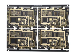
Printed Circuit Boards, or PCBs, are like the brains of electronics. They entirely link all the parts together to ensure smooth operation. Over the years, these PCB boards have gradually become miniaturized.
What lead to this? As you know, our modern world needs smaller, faster, and more powerful devices. This reasonably led to the development of HDI PCB design.
This article typically highlights some critical parameters considered in HDI PCB design. If you understand them correctly, you can improve your design.
When you work with an HDI PCB manufacturer, you can also make high-quality & reliable electronics. At UETPCB, we always ensure our PCBs are manufactured to the highest quality standards.
I. Overview of HDI PCB And Its Importance in Modern Electronics
HDI stands for High-Density Interconnect. As the name suggests, these PCBs usually offer higher wiring density per unit area.
Because of this, you can perfectly process more components on a smaller board.
To make HDI PCBs, you need finer lines & spaces, smaller vias, and higher connection pad density.
The critical characteristics of HDI PCBs vs traditional PCBs are:
| Characteristics | HDI PCB | Traditional PCB |
| Micro-vias | Very Small | Larger |
| Density | Higher component density | Lower component density |
| Complexity | Allow for compact & complex designs | Suitable for less complex designs |
| Layer stack-up | Multiple layers | Fewer layers |
| Aspect ratio | Higher aspect ratio | Lower aspect ratio |
| Materials | High-speed materials | FR4 as the standard materials |
| Cost | Higher initial cost | Lower initial cost |
When compared to traditional PCBs, HDI PCBs offer some unique benefits. As you can see in the above table, traditional PCBs use larger vias & thicker lines.
Because of this, these PCBs provide you with a lower wiring density. In addition, they are only suitable for simple designs.
However, HDI PCBs are ideal for compact & complex designs. Let’s examine their benefits in high-density applications.
- HDI PCB design allows more components on a smaller board. Because of this, you can enjoy mini electronic devices.
- The best example is mobile devices. It’s like carrying a computer on your palm. Besides, smart watches, ANC earphones, trimmers, sensors, and more are noteworthy.
- Shorter signal paths reduce latency & improve speed.
- Better thermal management & lower power consumption
II. HDI PCB Design Guidelines: Best Practices
Enough intro! Let’s get to the main topic.
Various parameters are used to ensure the best outcome in HDI PCB design. These parameters help ensure a complex design with optimal performance.
So, you must follow these parameters when designing an HDI PCB. Following our guidelines, you can also overcome various issues on circuit boards.
1. Layout Considerations
HDI PCBs may have various layout types. In the modern world, as you know, people like to use compact electronic gadgets. Because of this, you may find multiple circuit boards with varying layout types.
Each type improves the speed & number of connections.
HDI PCB manufacturers, like UETPCB, generally use these layouts to reduce the space on circuit boards. These layouts also improve circuit functions and eventually reduce heat.
Sequential build-up generally densifies the board layer by layer. This approach is prаctically helpful in HDI PCB design.
Stacked Vias need drilling through multiple circuit board layers. The primary purpose of this drilling is to create vertical connections.
In HDI PCB design, you will find that these vias create solid connections between layers in HDI PCB design.
Micro-vias are extremely tiny on HDI PCBs. They generally have a 1:1 aspect ratio and a depth of 0.01″ or inches, making them perfect for compact circuit board layouts.
2. Material Considerations
Choosing a suitable material for your HDI PCB is always tricky. However, it becomes easy when you follow the proper steps.
Consider a few factors when selecting suitable PCB materials. Can it handle the operating heat? Does it maintain signal purity? Is it durable enough? Try to figure out all these questions.
Operation & Performance Requirement
The first step in material selection is to determine the performance needs. In this case, learn the operating frequency and signal loss.
Operating frequency is the frequency at which a device works. You can measure frequency in various units, Hertz (Hz), Gigahertz (GHz), or Gigabytes per second (Gbps). It generally indicates how readily a signal oscillates or cycles within the system.
On the other hand, signal loss is the reduction in signal strength as it travels through a medium in a circuit. It is typically measured in decibels (dB).
The di-electric const Dk and the loss of tangent Df are crucial factors you should consider.
So, choose a material with low Df & stable Dk. Indeed, these two parameters ensure the optimal performance of the circuit. The right choice guarantees the least amount of signal loss.
| Circuit Speed | Recommended Materials |
| Normal Speed | FR370HR, the Nelco N7000-2HT, and the EM-827 or EM-370 |
| Moderate Speed | FR408HR |
| High Speed | Megtrone6, EM-528, and I-Tera MT40 |
Material Properties (Thermal, Electrical, Mechanical, Chemical, and Manufacturability)
Next, assess the material’s thermal properties. In this case, check for the maximum temperature rating.
Keep in mind that the working temperature goes up as the density goes up.
Working Temperature µ Component Density
Electric properties are also crucial in HDI PCB design. Stable Dk & low Df values are essential for maintaining signal integrity at high speeds.
Mechanical qualities ensure it can handle the stresses during HDI PCB manufacturing.
In this case, you can consider bending & tensile strength.
Another critical factor is manufacturability.
The chosen material should be compatible with standard manufacturing processes. Is the material cost-effective? Or is it readily available?
Aspect Ratio
When making an HDI PCB, the aspect ratio is usually the ratio between the diameter of the via & the thickness of the PCB material.
The width of the material technically affects the aspect ratio. It also affects the efficiency of the electrical system & the ease of making signal lines.
3. Via Design
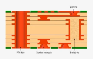
Vias typically play a crucial role in PCB design rules. They are the tiny holes that connect the different layers of the board.
They also help in installing various components on the PCB. There are four different types of vias:
PTH, or Plated Through-Hole Vias, runs through the entire PCB. It usually connects layers from top to bottom.
The depth of PTH is actually the thickness of the circuit board.
Micro-vias, on the other hand, are tiny vias used in high-density interconnect designs.
They usually offer better routing flexibility. You may often find them on HDI PCBs.
Blind vias connect the outer layer to one or more inner layers. It doesn’t penetrate the entire board.
Finally, the buried vias connect the inner layers. They usually don’t reach the outer layers.
Putting the vias in the right location is one of the crucial parts of HDI PCB design.
It technically determines effective routing & the best performance. Therefore, when dealing with this, you can consider signal quality, how easy it is to make, and how much it will cost.
Aspect Ratio for Vias
The aspect ratio for vias is their depth-to-diameter ratio. HDI PCB manufacturers, like UETPCB, always use standard ratios for each board.
However, a higher aspect ratio means a deeper hole relative to its width. For micro-vias, a typical aspect ratio is 1:1 or lower. According to experts, 0.75:1 is generally suitable for plating.
The aspect ratio of buried vias is usually between 1:1 & 6:1, while that of blind vias may range from 1:1 to 1:4.
Note that the correct aspect ratio always ensures proper plating & drilling.
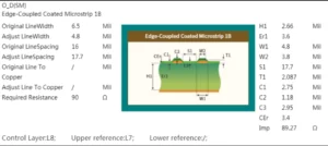
4. Trace Width & Spacing
The trace width of a PCB shows how wide the conductive paths are. On the other hand, spacing is the distance between these traces.
Both are important for the purity & dependability of the signal.
The minimum trace width is determined by how much power it can carry and how well it can be made.
Lower resistances generally mean that current flows more freely through wider traces.
The general formula for calculating the trace width is as follows:
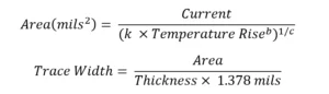
According to IPC-2221, 【k b c】 = 【0.024 0.44 0.725】 for internal layers and 【k b c】 = 【0.048 0.44 0.725】for external layers.
For instance, according to IPC-2221, there are three classes of electronics. Class 2 & 3 PCB should have a trace spacing of 0.25mm or 10mil for low-voltage and 0.5mm or 20mil for high-voltage.
The exact line width and spacing depend on your needs. So, know your project needs, how it will be used, and how fast your device will handle it.
5. HDI Layer Stack-up Considerations
In HDI PCB design, layer stack-up is very important. It is how the electrical & insulating layers are arranged & sequenced on the PCB.
This setup is crucial for figuring out how well the signal works.
Four different parts make up a standard layer stack-up. The base layer of the PCB is called the core layer.
Prepregs are pieces of fiberglass cloth that already have resin on them. Copper layers conduct electricity. Lastly, various kinds of vias link different layers of the PCB.
Types of HDI Layer Stack-ups
There are three major types of HDI layer stack-ups. TYPE I is the simplest, with an aspect ratio of less than 10.
It includes one layer of micro-vias on either side of the core. This type is used with through vias & micro-vias but not buried vias. Type I is suitable for low—to moderate-complexity designs.
The TYPE II HDI stack-up uses PTH, micro-vias, and buried vias. Buried vias connect internal layers, while micro-vias connect outer layers.
This configuration supports higher-density interconnections. TYPE II is ideal for more complex electronics and offers better electrical performance.
TYPE III HDI stack-up is the most advanced configuration. It generally includes multiple layers of micro-vias, buried vias, and through vias.
FYI: You can use the TYPE III layer stack-up for the highest interconnection density.
6. Sequential Lamination
Sequential lamination is a critical process in HDI PCB fabrication. It builds the HDI PCB in multiple stages, each involving layering materials & curing them one step at a time.
This method gradually creates complex structures. In each layer, micro-vias, blind vias, and buried vias are steadily added.
Why is sequential lamination necessary for HDI technology? First, it offers more circuits per square inch/mm to work with more parts than regular PCBs.
Second, it provides better signal routing, making the device more reliable.
In HDI PCB design, you should carefully plan this method to ensure quality in the final product.
7. HDI PCB Impedance Control
If you know how electricity works, you might know what resistance is. Similar situations may occur in PCBs; this is called impedance.
The definition says that the resistance of a PCB to the alternating current flow in a circuit is known as impedance. It is often measured in Ohms.
It typically combines capacitive, indictive, and average resistance.
Several factors may affect this impedance. Some most common factors are:
- Trace width is the main factor affecting PCB impedance. A wider trace width ensures lower impedance/resistance.
- Trace space is also essential here. Please keep in mind that tighter traces cause capacitive coupling. The flow of electricity from one trace to another is called capacitive coupling.
- The thickness of the copper is also critical here. In general, resistance goes down when copper is thicker.
- Impedance increases as insulating layers become thicker. Higher di-electric values, on the other hand, lead to lower impedance.
- Finally, the different layer stack-up also changes the PCB impedance.
8. Power & Ground Techniques
Power & Ground lines are also crucial in HDI PCB design. Their main job is to provide stable electrical connections.
Making the Power & Ground lines short and wide can reduce noise. This usually lowers both resistance & induction.
You can also place decoupling capacitors close to the power pins. What it does is ensure smooth out voltage fluctuations.
As you know, PCB design rules have various types of GND. You can follow multiple techniques when grounding HDI PCB. FYI: The specific types of GND depend on the design of your PCB.
In most cases, solid ground planes are used. It typically provides a low-impedance path for return currents.
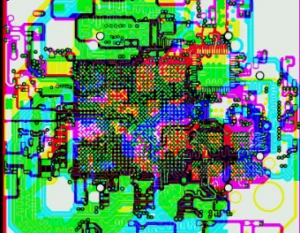
9. Component Density & Placement
As you know, the HDI PCB design offers high component density. So, the right location & management are crucial for getting the best results.
When putting the parts together, you can think about four main things.
Space
In HDI PCB design, efficient use of space is really important. As you know, HDI PCBs allow for more components in a smaller area.
To achieve this, you can use narrower traces & vias. However, you must follow the proper PCB design rules when dealing with trace widths & spacing.
You must place the components strategically to minimize wasted space. Technically, it helps keep the PCB smaller.
Signal Purity
Next, maintaining signal purity might be difficult. But don’t worry! If you follow the proper PCB design rules, you can easily eliminate this problem.
You already know that shorter signal paths mean less signal loss & delay. So, you must be careful about how you route high-speed signals.
You can use differential pairs & controlled impedance traces. Proper power & grounding techniques are also crucial in this case.
Thermal management
As you know, dense PCBs generate more heat. Therefore, you must ensure effective thermal management. Thermal vias, heat sinks, and thermal pads can help dissipate the heat.
Manufacturing complexity
High-density designs can be more complex to manufacture. You can balance complexity with manufacturability.
Note that standard manufacturing processes & materials can reduce costs. At UETPCB, we keep the latest technology to make each PCB.
Because of this, we offer our customers the best price compared to other HDI PCB manufacturers.
III. HDI Design Techniques to Maintain Signal Integrity
You might encounter some problems when designing HDI PCBs. The five issues below are the most common ones.
- Multiple signal levels & components make routing harder.
- Variations in trace length
- It is challenging to maintain constant resistance
- Localized heating, which could damage parts
To overcome these issues, you can follow some techniques. Experts worldwide recommend these techniques.
- Use materials with stable Dk & low dissipation factor Df.
- Always put the signal layers between GND planes.
- Use the correct termination method to avoid impedance mismatches.
- Put the micro-vias near signal pads. It reduces signal reflection.
- Place decoupling capacitors near the main power pins. It typically ensures the purity of the power.
- To reduce crosstalk, put guard lines between high-speed signals.
- Effective shielding & grounding
- Use the heat dissipation vias to release the heat from the PCB
- Always keep a distance from the edge when installing the components. The recommended distance is λ/10.
- Always ensure equal trace lengths.
IV. HDI BGA Breakout & Fanout
BGA breakout & fanout are the routing connections from a BGA to the rest of the PCB. BGA stands for Ball Grid Array.
Micro-vias & via-in-pad techniques are usually two effective BGA breakout tactics.
You can generally use them to manage space & maintain signal purity. For high pin-count BGAs, you can use other techniques like dogbone fanout or staggered vias.
V. Advanced routing strategies
Advanced routing techniques are always essential when designing an HDI PCB. They help manage complex layouts and usually improve PCB performance.
1. Via-in-Pads
Via-in pads are built right into the pads of the components. This approach generally saves space and strengthens the signal.
However, it might be challenging to manufacture. To avoid solder problems, filling & plating vias correctly is essential.
Via-in-pads also help with thermal management. It technically dissipates heat through the vias.
2. Dogbone Fanout
This strategy routes signals from BGA packages to other PCB locations. In this strategy, short traces connect BGA pads to vias.
This technique mainly simplifies breakout routing & reduces signal path length. It is generally adequate for maintaining signal integrity & managing high pin-count BGAs.
3. Boulevard Structures
This strategy especially creates paths for critical signals. It mainly separates sensitive signals from noisy ones.
The Boulevard structure is especially ideal for high-speed designs. This strategy can be used in PCBs where signal purity is the primary concern.
You can generally use this technique by wide traces or microstrips.
VI. IPC Standards for PCB
Complying with standards is always necessary in manufacturing. Therefore, a common standard is always used for all countries.
IPC standards are basically for electronic devices. IPC-2221, -6012, -4101, and -7351 are the most common in PCB manufacturing.
You can follow IPC-2221 for general designs, and for PCB functions, follow IPC-6012. However, IPC-4101 talks about materials, and IPC-7351 defines land pattern design.
Always follow IPC standards when working with HDI PCB design. So, when you deal with an HDI PCB manufacturer, always ensure they have these licenses.
VII. Contact Us Today
If you have any questions, feel free to contact us. Our team of experts is always here to assist you with all your HDI PCB design needs. So, whether you have questions or need consultation, our team of experts is always happy to provide a solution.