PCBs are the brains of electronics. They handle everything in an electronic gadget. From iPhones to hospital equipment, you need them everywhere. Therefore, making them must be professional and accurate. This is where the professional PCB assembly process comes in. Every step here needs testing and checking.
A printed circuit board assembly connects all the parts on a PCB. It is an essential step in making high-quality electronics.
You may have already observed that we are getting newer technology every year. Things are getting smaller and more complex. Because of this, people can do high-quality work efficiently. This change usually leads to high-quality PCB assembly processes. After all, we all want goods to work perfectly, and well-assembled PCBs make that possible.
Overview of Assembling Circuit Boards
Simply put, PCB assembly is the process of mounting electronic components. The tiny things you see on PCBs are the main functional components. The method of putting them in the right place is called PCB assembly. And, of course, it is the most critical part of manufacturing.
So, how you put the components on the PCB matters a lot. PCB factories generally employ different approaches. Each of these PCB assembly processes has unique benefits. Indeed, some are very accurate, while others offer cheaper solutions.
Through Hole PCB Assembly
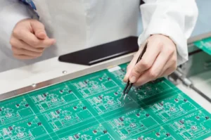
Through-hole or TH, PCB assembly is the most common method in PCB manufacturing. As the name suggests, the PCB components are connected using the holes and the leads of the components.
SMT Assembly
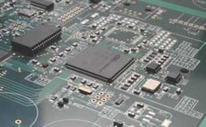
The SMT PCB assembly process is another great way to connect components. However, you are only limited to connecting components on the surface. With this method, you don’t have to worry about making holes because it only puts parts on the PCB surface. This method usually allows you to use smaller parts very quickly.
BGA Assembly
This PCB assembly process is fascinating. It is called BGA assembly, which stands for ball grid array. This approach links parts using tiny solder balls. Microprocessors and chips are all good examples of BGA assembly.
Wave Soldering and Mixed Assembly
The wave soldering method uses a solder wave to join the through-hole parts. This method is very effective for simple PCB assembly. Finally, the mixed PCB assembly may have all PCB assembly processes. The computer motherboard is the best example of a mixed assembly product.
Design for Assembly of DFM Strategies
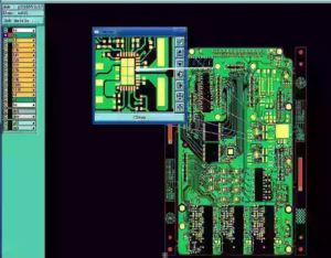
Intelligent design saves time and money, and PCB manufacturing is no exception. The most common terms used in PCB factories are DFA (Design for Assembly) and DFM (Design for Manufacturing). These two terms are generally the standards of PCB manufacturing. Using both these standards makes your PCB design highly efficient and optimizes the costs.
This is usually the case with DFA because it simplifies the building process and eliminates costs occasioned by errors. On the other hand, DFM usually checks that your plan works with how things are made. Putting these two together will ensure that your PCB assembly plan works well and has no mistakes.
When designing, there are many rules you have to follow. Among them, three key points are crucial. The first is proper assembly planning. It must be well-planned to make production faster and reduce costs. Second, the trace width must be clear, and signal traces must have short, straight lines. And third is the penalization and fiducial marks.
Getting Ready And Setting Up
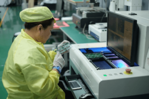
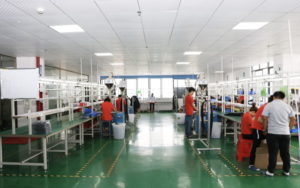
If you visit a PCB factory, you will find that the assembly lines are very organized. There’s a moving conveyor on which the PCB goes from one place to another. In each assembly section, one operator does their respective job. There’s checking staff as well. Each assembly line section has a box where the PCB components are stored.
An operator is assigned to ensure that all these boxes are full. He/she typically handles assembly design, plans, material lists, and bills of orders. Among his responsibilities, his main job is to check whether the necessary raw materials are ready for assembly. When choosing the right factory, you must ensure their capabilities of components sourcing.
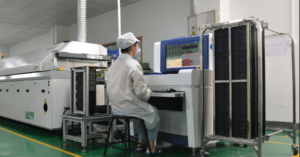
SMT Assembly Process with Automated Machines
SMT stands for surface mount technology. It is the opposite technical of TH assembly. In this method, you don’t need to drill holes. However, each component is soldered on the PCB, providing a direct mounting method. As a result, assembling SMT PCB is far more efficient and faster.
Automated SMT machines are high-speed and precise. They place thousands of components per hour. If you did that by yourself, it might take a few days. These machines also reduce human error. With SMT, you can control high quality and spend less on labor expenses.
In the SMT assembly method, there’s no hassle of putting component leads. This whole method is fully automated. It starts by preparing the solder paste. Then, an automated machine picks and places the components in the correct place. Finally, when you heat the PCB, the components automatically go to their designated places. As you can see, there’s no need for human touch. Therefore, you will find no errors and ensure high accuracy in the final product.
Through-Hole Component Insertion PCB Assembly Process: Step-by-Step
The SMT PCB manufacturing method is only suitable for surface-mount tasks. However, through-hole component placement is a different approach. This PCB is used in most electrical and electronic devices but not high-performance gadgets.
Preparing the PCB and Components for TH PCB assembly
The room where the PCBs are assembled must be clean and dust-free. If you go to a PCB factory like UETPCB, you will see that the production line has good ways to keep dust out.
This step is important because dirt can interfere with the electrical signals between the PCB components. The through holes are checked for TH PCB construction to ensure they are lined up. Another person verifies the hole size to match the leads of specific components.
Manual or Automated Insertion
When everything is set, the insertion process is typically achieved in two methods. Manual operation is slow but highly suitable for sensitive equipment. Prototypes, high-value or sensitive, and mixed-technology PCBs usually require manual insertion. On the other hand, automated insertion is ideal for bulk products and significantly larger boards.
In this step, the overall work is to place the leads of the components through the existing holes. Whatever technique you use, you must ensure that the leads of these components sit flush with the board. The operator or machine bends the leads slightly by hand to help hold the components.
Soldering the components
It’s now time to strengthen the PCB’s parts. To do this, you will need to solder. Different production lines in factories use different soldering techniques. Three soldering techniques are the most common in modern factories.
In wave soldering, the liquid solder finish is normally employed to reveal the leads and pads. This method works well for making a lot of things at once. On the other hand, selective soldering is ideal for mixed technology. The operator solders the selective places. However, manual soldering is only suitable for making prototypes or small-scale orders.
Visual Checking and Cutting of Extra Leads
In the previous steps, you bent the long leads of the components just a bit. After soldering, you must remove this extra part. Otherwise, it may interfere with the electrical signal.
Types of Testings in PCB Assembly Processes
Every PCB factory performs thorough testing throughout the whole PCB assembly process. Without it, the chances of failure are high. UETPCB factory is no exception. They usually perform two major types of testing.
Inspection and Quality Check
Visual inspection and general quality checking are standard PCB testing processes. They are widely used in both factories and repair shops.
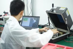
One of the most common is AOI or automated optical inspection. This machine uses a camera to check whether the components are placed correctly. X-ray is another machine used in quality checks. It finds hidden solder joints and helps identify cracks, voids, or internal problems.
UETPCB also performs other manual checks to ensure the highest quality of the PCB.
Functional Testing
Functional testing machines are not regular items. You won’t find them in nearby repair shops. As you know, people use circuit boards in diverse environments. So, functionality testing in those environments is crucial.
Like in marine, moisture is a common threat. So, if you make PCB for marine situations, you must check whether it can handle such moisture levels. A similar checking is also performed for vibrations and temperatures.
Post Assembly
After assembly, every PCB must be cleaned to remove flux and debris. As you know, working on every PCB panel requires time and costs. Engineers solved this issue by implementing the panelization technique. This approach generally allows multiple PCB assemblies on a single large panel.
After the assembly, you must remove these small panels from the large ones. Some residue remains, which needs to be cleaned later. You must trim them to ensure a better fit in the final device.
The packaging also plays a critical role in the PCB manufacturing process. Various companies worldwide are the main customers of these PCBs. Therefore, the packaging must withstand the stress of international shipping. UETPCB ensures high-quality packaging and 100% safe delivery to any country worldwide.
China Printed Circuit Board Assembly
China is a great place to make PCBs, and UETPCB is the leader in this industry. Among other PCB assembly manufacturers in China, UETPCB has earned a remarkable position in 2024. Chinese PCB makers can help you save money without lowering the quality of your work. The main reason behind this cost-effectiveness is China’s low labor cost.
Please contact us if you have any questions or want to learn more about the PCB assembly process. We have a very professional team of experts who are always happy to assist you.

