
“With Rigid-Flex PCB, the future of electronics is both flexible and strong.” We are all more or less familiar with PCB. You know, it stands for Printed circuit board. Every day, our world is evolving. People demand more convenient electronic gadgets. This high demand creates different types of PCB: rigid, flexible, and rigid-flex PCB.
Rigid-flex PCBs have both stationary and flexible parts. This means you can enjoy both features at the same time. As a result, this PCB opens up a vast opportunity to make unique electronic gadgets. This article will highlight the fundamentals of this PCB. We will mainly focus on how a rigid-flex PCB is made. To make the discussion simple, we will go through a step-by-step process.
What is Rigid-Flex PCB?
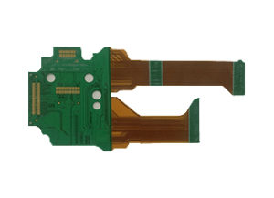
A rigid-flex PCB is a type of printed circuit board. As the name suggests, it combines the features of rigid and flexible circuits. So, you can bend it and maintain the rigid part at a time. Because of these dual features, rigid-flex PCB is preferred in many applications.
The construction of rigid-flex PCBs is as typical as that of rigid and flexible PCBs. The flexible part has a polyamide base, while the rigid part has FR4 boards. The PCB fabrication connects these layers using PTH (Plated Through Hole).
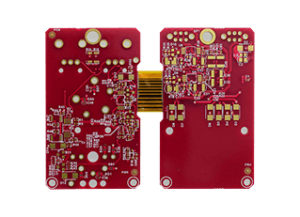
Rigid-flex PCBs are prevalent in various uses. They can be found in consumer electronics, medical devices, automotive systems, and more. Typical products are smartphones, tablets, laptops, car navigation, and control systems.
Why are Rigid-flex PCBs so Famous in the Electronic Industry?
There are several reasons why rigid-flex PCB is so famous in the electronic industry. As you know, it has both rigid and flexible PCB features. Combining all these features, you can enjoy the following few benefits.
#1 Space-Saving
The best part of a rigid-flex PCB is that it is space-saving. They usually offer a three-dimensional configuration. You can fold or bend it, whatever you like to do. You can also independently install these PCBs on your gadget to reduce size. Moreover, your gadget becomes more lightweight and compact.
#2 Design Flexibility
Rigid-flex PCB offers remarkable design flexibility. You can shape it to fit any complex geometries. Most importantly, these PCBs can give you dynamic bending. As you know, this is very important for moving parts. So, a rigid-flex PCB allows you to design these moving parts more efficiently.
#3 Reliable Connection
Another significant benefit is the reliable connection between components. When you use rigid-flex PCB, you don’t need connectors or cables. It eliminates the extra connection hassle. As a result, you can get a reliable connection.
#4 Simple Assembly
Rigid-flex PCB simplifies the assembly process. It needs fewer components and connections, so it gives a quick assembly. Since the rigid-flex board is easy to install, there’s almost no possibility of errors being made.
#5 Improved performance
A rigid-flex PCB can handle high-frequency signals with less interference. Its integrated design reduced the need for connectors. In addition, these PCBs also allow you to make simple assemblies. Considering all these benefits means lower electrical resistance and better overall performance.
#6 Long-life
A Flex-rigid PCB can fix the problems with contact and extreme heat that cables and connectors cause. As a result, these characteristics dramatically improve device reliability. Overall, rigid-flex PCBs last a long time. Their sturdy shape lets them bend and flex over and over again. You must ensure the design and materials are correctly chosen when making PCBs.
Rigid-Flex PCB Fabrication Process: A Detailed Step-by-Step Process
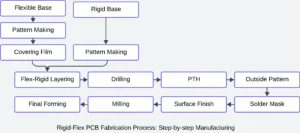
Rigid-flex circuit board manufacturing has several steps. Since it combines rigid and flex, the PCB-making steps are also detailed. UETPCB always ensures top-notch quality circuit board manufacturing. Thus, UETPCB rigid-flex circuit boards are world-class standards.
Step #1 Rigid-Flex PCB Design and Simulation
The first step is designing the rigid-flex board. Altium and Cadence are widely used to design PCBs in the real world. When designing layer stacks, flex-to-rigid transitions and component placement matter the most. After designing, we also simulate the whole product. We check signal quality, produced heat, and mechanical stresses.
Step #2 Preparation of Base Material for Flex PCB
The quality of a flex PCB depends heavily on the base material, which is a thin and flexible polymer layer. Polyamide is often used as the base material for flex PCBs, but PET could also be used.
The base material is first cleaned and made ready for flex PCB production. Adhesives are then used to stick the copper foil to the surface.
Step #3 Pattern Generation for Flex PCB
As the name suggests, this step involves creating a pattern on a flex PCB. In this case, you need to know about photolithography.
Photolithography is the process of producing circuit patterns on flexible PCBs. It must be precise. Otherwise, there’s a chance of a short circuit or heat generation. Film and etching methods are used for this job. In this situation, etching eliminates extra copper and leaves a precise pattern.
Step #4 Covering Film for Flex PCB
After photolithography, we apply an overlay or solder mask to the flex PCB. Curing is also necessary to ensure perfect adhesion and protection. We will send the flex PCBs to the testing lab when this stage is complete. After testing, the flex PCBs are ready to be layered with the rigid PCB.
Step #5 Preparation of Base Material for Rigid PCB
This step also prepares the base material for rigid PCBs like flex PCBs. FR-4 is widely popular for this job. We also clean and prepare the base material for copper cladding.
Copper cladding is a process of bonding a thin copper layer onto the surface of the base material. UTPCB always gives special attention to this step. Proper preparation ensures the quality of the PCB.
Step #6 Pattern Generation of Rigid PCB
Like flexible PCBs, rigid PCBs also go through a process called photolithography. As you know, this step is very important for rigid PCB to work accurately. UETPCB always performs quality checks at this stage to prevent errors. Once testing is done, our rigid PCB is ready for layering.
Step #7 Flex-Rigid Layering Up
This step combines flexible and rigid PCB, hence the name rigid-flex PCB. First, we align and laminate the flexible and rigid layers. Then, we apply firm pressure and heat to bond the layers securely. We attach a specific part of the flex PCB based on our design.
Step #8 Mechanical Drilling
Drilling creates interconnectivity in circuit board manufacturing. Most of the time, we use CNC drilling machines for this purpose. To ensure accurate placement, we also use precise measurement tools.
After drilling, we check whether the drilled hole is accurate. Next, we clean debris and burrs from the hole. In this case, we use high-pressure air and brushes.
Step #9 Through Hole Plating
PTH, or Plating Through Hole, creates a conductive path between layers. In the previous steps, we drilled and created holes. To make the PTH, we use electroless copper plating, which makes the inner wall of the hole conductive. Once done, we rinse and dry it to remove residual chemicals.
Step #10 External Pattern Generation
In this step, we will create the outermost layer of rigid-flex PCB. Once again, we will use the photolithography process to make the external patterns. For precise patterns, we will use the etching technique.
Step #11 Solder Mask
The main purpose of a solder mask is to protect the circuit pattern from oxidation. It’s a thin polymer layer with a greenish color. People also call it “solder resist” or “solder stop.”
We use the screen printing method to apply a solder mask over circuit patterns. Then, we cure the mask under UV light to harden it.
Step #12 Surface Finish
We do surface finishing in many ways. It mainly depends on the type of PCBs. We often use OSP, ENIG, immersion silver, immersion tin, hard gold, and soft gold.
Step #13 Milling
This step is necessary to create various cutouts and slots for components. We mainly use CNC milling to route and cut PCBs to their required shapes.
Step #14 Forming
Finally, we perform some last shaping processes to fit design specs. Once done, we move our rigid-flex PCB to the testing lab. Once testing is done, we complete the rigid-flex PCB fabrication.
Frequently Asked Question
What is the difference between rigid-flex and flex PCB?
A Rigid-flex PCB combines both rigid and flexible circuit boards. Only rigid PCBs are stiff and stationary. They are simple and thicker than flex PCBs. Conversely, flex PCBs are thin and bendable. Rigid-flex PCB is both bendable and robust.
What material is used in rigid flex PCB?
Since rigid-flex PCB combines two types of PCBs, it uses two materials. Polyimide is prevalent for flexible PCBs, and FR-4 is for rigid ones. This combination makes rigid-flex PCBs more durable.
What are the examples of rigid-flex?
Rigid-flex PCBs are prevalent in many different places. Smartphones, digital cameras, and robots stand out as portable gadgets. Various moving parts in manufacturing machinery need these PCBs. In addition, they have thousands of uses in cars and airplanes.
Summary
Rigid-flex PCB fabrication involves several steps. It begins with the design and simulation of the whole PCB. Then, separately, rigid PCB and flexible PCB are made. Later, step 7 layers up these two separate PCBs.
Steps 8 and 9 create various holes in the PCB. Step 10 generates the external pattern. To protect these patterns, step 11 creates the solder mask. Step 12 gives surface finishes, while steps 13 and 14 finalize the board’s structure.
UETPCB is a leading manufacturer of rigid-flex PCBs. If you have questions regarding the PCB manufacturer, please contact us. We have a team of experts who are always happy to answer your questions.