
This helpful article is for anyone who has encountered the terms bare boards or zero PCBs. Learn their meanings and how useful they can be for your prototypes and designs.
Introduction
You’ll usually need a lot of test work before arriving at a finished electronic product. Along the way, you may need a lot of prototyping and testing tools. With this, you may come across the terms zero and bare PCBs. These boards are usually indispensable during the design process.
At first, you may find a breadboard fits most of your initial prototypes. However, a breadboard will always have its shortcomings. Breadboard connections are temporary, easy to take apart, and don’t consider circuit layout constraints. At most, breadboards help verify your circuits at a functional level.
Where do Zero PCBs come into Play?
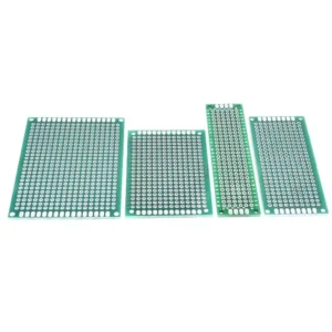
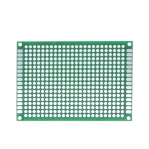
Zero PCBs are boards populated with copper donut holes that don’t have a predefined circuit layout. The designer creates the tracks to connect these holes. As you may guess, zero PCBs function much like a breadboard; only you’ll need to solder and join the components together through the donut holes on the board.
Zero PCBs come in different shapes, sizes, colors, and compositions. Most users find them sold in electronic hobby shops.
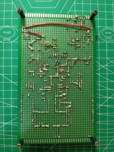
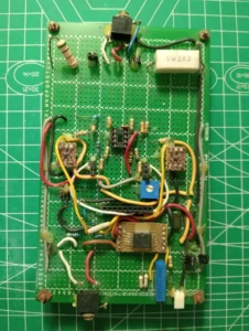
Below is an example of a zero PCB with soldered components. Notice that some donut holes are soldered together to create circuit tracks.
Different Kinds of Zero PCBs
You’ll usually see two variants of zero PCBs: brown and green. The green variant looks a bit more elegant to work with than the brown variant, for reasons you’ll see below.
FR1 Zero PCBs
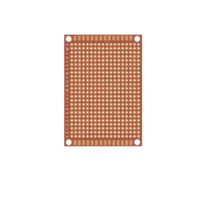
If you want to save on costs, you can use the brown-colored variant, which most people also call FR1 (or commonly called paper) PCBs. FR1 stands for Flame Retardant 1. FR1 comprises Phenolic Paper Laminate (hence the name paper PCB). You’ll usually find FR1 used on single-sided PCBs on cheap electronic products such as chargers or adapter boards.
Many school projects use FR1 zero board PCBs for their main boards during their introductory electronic courses.
FR4 Zero PCBs
One of the more common and sturdier materials used in PCB manufacturing is the standard FR4 PCB. FR4 PCBs have FR4 (Flame Retardant 4) material as dielectric and are composed of glass fiber cloth and epoxy resin. FR4s are more durable and have higher working temperatures than their FR1 counterparts.
With the characteristics mentioned above, FR4 zero PCBs are perfect as prototyping materials for various applications, including logic, power, RF, telecom, and more.
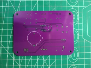
Where do Bare PCBs come into Play?
You’ll always have batches of PCBs with a circuit layout during the design process. Initially, these PCBs don’t have components on them, so they are called bare PCBs. Bare PCBs have all the necessary detail layers to populate your board with components. These detail layers comprise the solder mask, silkscreen, and foil pattern layers. Users may find assembling the board with components and information regarding these detail layers easier.
A user should design a bare PCB before manufacturing it. A designer usually uses a CAD program to create the board. Such programs include KiCAD, Cadence, OrCAD, EasyEDA, and Fusion. After this, the user generates manufacturing files. These manufacturing files (fabrication outputs) are usually in Gerber format. A PCB fabrication house typically requires Gerber files to manufacture the zero PCBs.
An assembled PCB is a PCB in which components are stuffed, placed, and soldered. People can do the assembly process manually or let a pick-and-place machine do it for them. It would make sense to have your PCBs assembled by a machine, especially if there are lots of PCBs involved.
Testing Bare Boards
After manufacturing, users should test bare boards thoroughly to ensure they are free of defects. The testing should include continuity and short-circuit checks. Fortunately, automated processes do the checks after the boards are manufactured. Below, you’ll find the different testing processes.
Fixture Test (In-Circuit Testing)
Fixture test or In-circuit testing (also called ICT) is a commonly used process for testing circuit boards. The process involves a mechanical fixture with a bed of nails. These beds of nails are test jigs (composed of electrically conductive pogo pins) that come in contact with the PCB’s actual circuit layout. Once in contact, electrical checks are made to determine if there are shorts, opens, or undesired connections on the boards.
It is best to prepare your bare PCB designs before undergoing a fixture test. To do this, you have to include physical test points on your boards. These points should match the corresponding pogo pin that will land on them. Sometimes, vias can be used as test points if they are compatible with the Pogo pins.
Flying Probe Test
When fixture tests can’t do the job, or you need more speed and precision, you can do a flying probe test. Flying probe tests are more flexible because a mechanical arm reaches through the test points for electrical checks. You can do this test even when components are in the way. Additionally, fabrication houses may find it costly and time-consuming to manufacture test jigs that aren’t needed for a flying probe test.
A Flying probe test consists of a robotic (CNC style) mechanical arm. The accuracy and speed of the arm determine the cost savings compared to an ICT test. A flying probe test is like a contactless point test and is generally safer compared to the impact or stress an ICT fixture can apply to your circuit boards.
Conclusion
You’ve learned about bare and zero PCBs. Basically, bare boards don’t have components assembled on them and come fresh from manufacturing. Zero PCBs are prototyping boards that test your circuits, which are more reliable and durable than breadboard circuits. You’ve also learned about different testing methodologies for testing manufactured boards.