
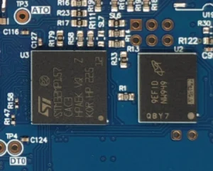
Knowing about ICs before learning about a QFN package is equally important. You may have found black, rectangular-shaped components if you have explored circuit boards. Yes, you guessed that right—they are ICs with packaging.
Integrated Circuits, or ICs, are the most important parts of modern PCBs. They can perform many complex functions, from amplifying signals to performing math. Many modern devices use this component. Typical examples include mobile devices, laptops, Desktop CPUs, cameras, and many more. Besides, regular gadgets like automated cleaners, WIFI routers, and many more are available.
Even though ICs are small, they are very robust. This robustness generally comes from special packaging. ICs consist of millions of transistors, which can do many complicated jobs. But this power comes with a price. During high peaks, they produce a lot of heat. This is why different types of packaging ICs are used.
People demand smaller, faster, and more efficient devices in the modern world. These features typically lead to increasing use of ICs and different packaging styles. Packaging has various roles. It mainly protects the ICs and helps dissipate heat. The QFN package primarily improves the performance of ICs.
The article will cover the fundamentals of the QFN package, how it works, and its advantages. We’ll also compare QFN and QFP, common on modern circuit boards.
What is the QFN Package?
The full form of QFN is Quad Flat No-Lead. The QFN package is the most popular type of IC packaging. “No-Lead” means that the QFN package has no protruding connection pins. Instead, the connections are found at the bottom. Because of this, this IC packaging is compact and low-profile.
What does the QFN package exactly do? Its main job is to protect ICs and dissipate heat. To do this, it provides a reliable and efficient way to house ICs. Also, the QFN package allows for better electrical performance. Because of this, they can be used in high-frequency applications. You will learn more about its functions in the later sections.
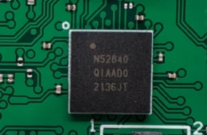
A QFN package is mainly black, square, or rectangular, with a flat surface and no visible leads on the sides. Instead, it uses a small pad for soldering on the bottom. Since it is located at the bottom, you can directly install it on the PCB.
There are varying QFN package sizes. Although it depends on the type and size of ICs, the typical size ranges from 3mm to 10mm per side.
The Structure of a QFN Package
A Quad Flat No-Lead (QFN) package has six main parts. Each part does a specific job and is very important to efficiency. This section will show them off and help you understand what they should do.
Die or QFN Chip
The semiconductor die is the core component of the QFN package. It is the QFN chip or IC. This component’s main purpose is to handle the actual job of the PCB. The die is typically made of silicone.
Die Attach
This component refers to the adhesive or solder used to attach the die to the lead frame. A reliable die attach is necessary to ensure optimal thermal and electrical pass.
Exposed Thermal Pad
This component is visible from the bottom side of the QFN package. Its main job is dissipating heat and ensuring the IC works properly. This component mainly determines the longevity of the die or IC.
Lead Frame
A lead frame is the main component distinguishing QFN and QFP packages. It connects the IC with the external circuit. The QFN package has no protruding pin, but you can see it below. Because of this, it is compact and low-profile.
Bond Wire
Bond wires connect the die to the lead frame, allowing electrical signals to pass between them. These thin wires, usually made of gold or aluminum, ensure reliable electrical performance.
Mold Cavity or Body
This part is one of the crucial parts of the QFN packaging. The black, square, or rectangular structure you see from the outside is the mold cavity or body. Epoxy is often used to make this mold because it is a good material for strengthening structures.
Advantages of the QFN Package
Quad Flat No-Lead frame offers several benefits. First, it’s small and flat. Second, it gives you better control over the temperature. Third, it’s simple to put together. Because of these three things, the QFN package works well with modern tech. Besides, the QFN package offers other benefits. Let’s check them out.
Enhanced Thermal Performance
The exposed thermal pad in QFN packages offers enhanced heat dissipation. Therefore, during operation, the IC can perform its job smoothly. Because of this, your IC lasts longer and does not need frequent replacements.
Compact Size
QFN packages are small and flat-shaped. They usually come in compact, low-profile sizes, which makes them lightweight. These size constraints allow you to create compact PCBs for more complex electronic gadgets.
Enhanced Electrical Performance
Since no protruding pin is used for QFN IC, it creates a short electrical path. This way, the component minimizes inductance and results in better signal quality. This feature is especially crucial for testing or computing equipment.
Simple Assembly Process
The QFN package is small and lightweight. It also doesn’t have any protruding pins that require extra assembly processes. Therefore, QFN packages are easy to assemble and reduce production costs.
Reliability
QFN package soldering creates a strong mechanical bond. Strong soldering is especially necessary for gadgets that involve vibration. It makes the PCB more reliable to the user.
Reduced Delamination
One of the best things about this IC package is its reduced delamination. Delamination is generally the unnecessary spacing on PCB boards. QFN packages save much space since they are square-shaped, flat, and have no protruding pins. They also allow for easy assembly of other components.
QFN Package Assembly Process
Every factory must ensure a controlled environment when conducting the assembly process. The QFN package has no protruding pins; thus, its soldering process is critical. In general, there are five major processes for assembling the QFN package. Each stage is critical to assuring the quality of the entire assembly process.
Applying Solder Paste
First, you can prepare solder paste to apply to the PCB in the right place. You could use a stencil to do this job. Always be careful at this stage. You must ensure the QFN IC has the right amount of solder for the assembly process.
Placing the Component
Then, properly align the QFN IC on the solder paste-deposited pads before placing it in its position. In most factories, automated pick-and-pick machinery is used. However, if you use it with your hand, carefully do this step. Note that proper alignment is vital for effective soldering.
Initial Inspection
After placing the IC, carefully check whether you did it right. You can look for three things here. (1) misalignment of the IC, (2) Wrong positioning, (3) insufficient contact between IC and solder phase.
Reflow Process or QFN Package Soldering
At this step, most factories place the PCB in an oven, where the solder paste melts and adheres to the QFN chip. This entire process occurs on the conveyor belt. If you do it yourself, you can use a standard heater. But make sure the epoxy body isn’t overheated.
Final Inspection
Check whether the QFN package soldering is done correctly one more time. You must conduct this stage after the assembly has cooled down. This step ensures that all the connections are secure and the assembly meets quality standards.
QFN VS QFP Package: Which is Better?
QFP stands for Quad Flat Package, while QFN stands for Quad Flat No-lead Package. They mainly differ in having leads. Both of them are widely used in the electronics industry. Having this extended lead has equal benefits and limitations. Because of this, QFP’s limitations become QFN’s advantages. Let’s learn more.
When is the QFN Package Preferred?
Since the QFN IC package doesn’t have extended leads, it is compact and low-profile. This package’s small size generally makes it suitable for compact PCBs, making it especially popular for making portable devices.
The exposed thermal pad also offers excellent heat dissipation. The no-leads feature generally shortens the electrical passes, improving signal quality. These packages are mostly used in high-frequency and sensitive equipment.
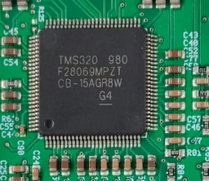
When is the QFP Package Better?
QFP packages, on the other hand, come with extended leads. This type of package is ideal for electronics that need high pin counts. Also, extended leads make it easier to visually check solder joints. However, QFP packages are bigger than QFN packages. They take up more space and are more prone to PCB delamination.
QFP packages greatly simplify soldering and reduce the likelihood of bridging. Soldering the extended joints creates more strong bonds than QFN package. Because of this, they are an excellent choice for uses on PCBs where mechanical strength is a concern. You may often find them used in larger or more robust systems.
Summary
Quad Flat No-lead package, or QFN package, is a widely used component for PCBs. It’s small and has a low profile. Also, this component is incredibly lightweight and flat. Because of all these features, the QFN package is ideal for compact and dense PCBs.
QFN packages are commonly used in complex PCBs. Typical examples include consumer electronics, telecommunication, and testing equipment. Compared to the QFP package, QFN offers better heat dissipation and signal quality.
Above all, if you are interested in creating custom PCBs, don’t hesitate to contact UETPCB customer service.