
Check this article for the critical differences between VCC, VEE, VDD, and VSS. Learn where these terms came from and their applications in practical electronics.
Introduction
Most likely, you’ve encountered one of the terms VCC, VEE, VDD, or VSS in your everyday encounter with electronics.
These symbols may have represented the power sources of your electronic circuits or ICs.
However, have you wondered about each specific character’s meaning in these symbols?
You’ll learn all about this here. You’ll also learn some practical applications employing these terms in your schematics.
What is VCC in full form in Electronics?
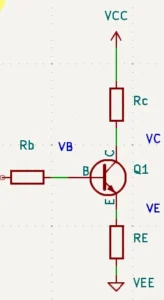
Designers generally use VCC in classic circuits with a bipolar junction transistor (BJT).
A BJT is a device used to amplify or control an electrical signal. It is mainly a current-controlled device.
As you’ll see below, a BJT is a three-terminal component with the pins collector (C), emitter (E), and base (B).
What’s unique about BJTs is that they should be biased to function appropriately. Generally, a typical configuration for a BJT is the common-emitter configuration.
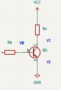
Looking closely at the circuit, one can see that its power source is VCC. It is believed that traditionally, the term VCC came from knowing that this source supplies the collector voltage or VC.
The double CC notation distinguishes VCC (the power supply of the collector of the transistor) from VC (the voltage at the collector pin).
However, you’ll also see the VCC symbol tied to the power pins of some ICs, especially the classic ones.
These chips employ an old (but tried and tested) manufacturing technology using BJTs.
Below is an example of a chip called the UA 741 operational amplifier from National Semiconductor.
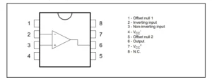
The internal construction of this IC is mainly composed of BJTs. The VCC pin is mostly connected to power the collector pins of the transistors in the circuit.
What is VEE in full form in Electronics?
Like VCC, VEE came about from another pin on the BJT called the emitter. The voltage on the emitter pin is VE or emitter voltage.
With this, the term VEE, which supplies power or ground to the emitter pin, was born to differentiate it from VE.
Usually, circuit layout engineers treat VEE as equal to ground in a basic common emitter configuration.
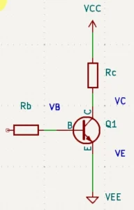
However, there are different kinds of configurations for the common emitter. One such configuration is an emitter-stabilized circuit.
Such a circuit has a resistor connected between the emitter pin and ground; thus, VEE and GND are unequal in this circuit.
Again, similar to VCC, you’ll find many classic chips with the VEE symbol as a power source.
These chips are generally internally constructed from BJTs. Usually, designers connect these pins to GND or a negative potential.
However, some chips differentiate the VEE terminal from the ground terminal by specifying that the VEE pin requires a negative supply voltage.
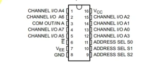
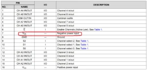
Here is an example of a chip called an analog multiplexer/demultiplexer circuit CD74HC4051.
If you have only a single supply voltage source and don’t need a negative potential, you should be able to connect VEE and GND.
What is VDD in full form in Electronics?
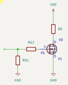
If VCC was born from BJT circuits, the term VDD came from FET (or Field Effect Transistor) circuits.
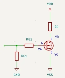
Like BJTs, designers mostly use FETs to amplify or control an electrical signal. FETs are components with three terminals: D for Drain, G for Gate, and S for Source.
Unlike BJTs, FETs are mainly voltage-controlled devices. FETS also have higher input impedances than their BJT counterpart.
Below is a simple FET (specifically, the MOSFET type) circuit. Looking closely, one can see that its power source is VDD, which powers the drain pin.
It is believed that traditionally, the term VDD came from knowing that this source supplies the drain voltage or VD.
The double DD notation distinguishes VDD (the power source of the drain of the transistor) from VD (the voltage at the drain pin).
Additionally, you’ll see the VDD symbol tied to the power pins of some ICs, especially the newer ones.
These chips employ a more efficient manufacturing technology using FETs. ICs made with FETs are more temperature stable, have a higher transistor packing density, and are easier to manufacture.
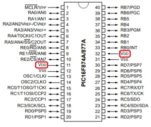
Below is an example of a chip, a microcontroller called PIC16F877A from Microchip Technology, that employs FET manufacturing techniques.
What is VSS in full form in Electronics?
Like VDD, VSS comes from another pin on the FET device called the source. The voltage on this source pin is called VS, or source voltage.
VSS supplies power or ground to this source pin. The double SS on the VSS term differentiates the VSS supply from VS or source voltage.
Note that VSS can equal ground in a basic N-channel FET configuration.
Again, similar to VDD, you’ll find many modern chips with the VSS symbol as a power source. Circuit designers usually connect these pins to GND or a negative potential.
As discussed earlier in the VDD term, these chips are generally internally constructed from modern FET technology.
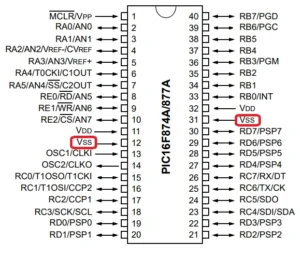
The example microcontroller IC PIC16F877A has VSS as its ground pin, as seen below.
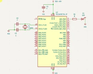
Employing this chip on a circuit will show you the connections between VDD and VSS. Below, the circuit applies +5V to VDD, which supplies it to the MCU’s VDD pins.
The circuit provides the MCU’s VSS pins with ground or zero potential. This example circuit blinks an LED using a microcontroller.
A firmware is additionally burned to the MCU to accomplish this task. Note that the circuit’s ground potential is all tied to VSS.
Conclusion
You’ve learned the terms VCC, VDD, VEE, and VSS here. Mostly, these are power supply pins that supply power to an electronic circuit or chip.
VCC was derived from the collector voltage of a BJT, VDD from the drain voltage of a FET, VEE from the emitter voltage of a BJT, and VSS from the source voltage of a FET.
Also remember that although VEE and VSS pins mostly connect to ground, they can also have a negative potential based on the application of your circuits.