
Electronic devices, such as smartphones and control display systems, have smaller electrical components. They offer powerful functionality but within a compact unit called a printed circuit board (PCB).
There are different types of PCBs. Among them, one of the best is the multilayer PCB, which is divided into multiple layers for circuit operations. They are compact, efficient, and provide superior functionality. Today, we will dive deep into multilayer PCB circuits and understand how they can help you out!!
What is a Multilayer PCB?
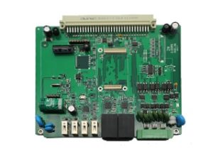
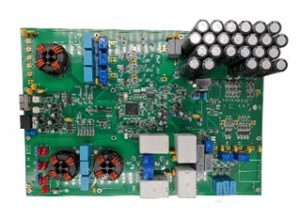
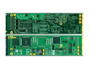
A multilayer PCB is a compact unit comprising multiple layers of copper traces separated by insulation. Compared to bilayer PCBs, they might have four, six, eight, or even more layers packed into a single circuit.
This typical structure includes the following components.
- Dedicated layers for the electrical routing and power transmission
- Special power planes provide easy and smooth voltage distribution throughout the system.
- For noise reduction, there are specialized ground planes.
- Insulation layers separates all the conductive layers from each other
- Vias connecting different layers and improving the overall density and strength.
Advantages of Multilayer PCBs
You might wonder why you should choose a multilayer PCB over a single-layer or bilayer PCB. There are several benefits discussed here.
High Density
Compact applications, such as smartphones or control displays, can’t afford large circuit sizes. Doing so can increase the device’s overall size.
However, a multilayer PCB offers advantages in such cases by accommodating multiple layers and circuit routing. Designers can create more layers and accomplish all the necessary tasks within the limited space.
The benefits include:
- Compact board size with all the required functionalities
- Better flexibility to place component with more options
- Support for miniaturized products
- Effective space utilization in the circuitry
Elevated Performance
The number of layers is essential for electrical performance. Compared to single- or bilayer PCBs, multilayer PCBs provide superior performance.
Dedicated sections for power and signals improve signal strength while reducing electrical noise and interference.
As a result, you could get higher electrical performance with the following benefits.
- Reduced electromagnetic interference (EMI)
- Lower signal distortion
- Improved signal quality
- Faster data transmission
- Better impedance control
High Reliability
Many industries rely on device reliability. A single-layer PCB is not as durable as a multiple-layer PCB.
Why? Because the bonding process and the circuit’s high density make it more reliable and improve overall performance.
Reliability benefits include:
- Strong structural integrity
- Reduced wiring complexity
- Fewer external connections
- Lower risk of connection failures
- Improved long-term performance
Compact Size
Modern circuits and technology are moving toward compact sizes. They can’t sacrifice quality and functionality for the sake of size. Therefore, options such as multilayer PCBs are the best choice at this point.
They feature more functionality yet in a small PCB unit. The compact size benefits are:
- Lightweight construction
- Reduced product thickness
- Compact device design
- Better portability
- Space-efficient assemblies
Effective Signal Integrity
Several factors affect the signals, such as interference and electrical noise. The smooth transmission of the signals is essential for effective results.
Multilayer PCBs offer design flexibility and allow engineers to place the ground and power planes close to the signal layers. This improves the signal strength and decreases interference.
Benefits of better signals include:
- Reduced crosstalk
- Controlled impedance
- Lower signal reflection
- Stable high-frequency performance
- Enhanced communication reliability
Flexible Design
Design freedom is a blessing in electrical circuits. Because of their smaller size and limited number of routes, bilayer PCBs don’t offer the same level of flexibility as multilayer PCBs. However, multiple layers of copper traces have enabled engineers to use this facility.
They can design and route the signals through multiple pathways. The flexibility includes:
- Easier routing of complex circuits
- Accommodation of high pin-count components
- Improved thermal management options
- Enhanced system integration
- Greater scalability for future upgrades
Thermal Management
In electronic devices, heat dissipation and management are major concerns. Whenever a circuit overheats, it fails to perform. However, a multilayer PCB handles heat very well by distributing and dissipating it across multiple copper layers.
The benefits include:
- Better heat spreading
- Reduced hot spots
- Enhanced component lifespan
- Improved system stability
- Support for high-power applications
Applications of Multilayer PCBs
Multilayer PCBs are crucial components of various industries discussed below.
Consumer Electronics
One of the best uses for multilayer PCBs is consumer electronics. They integrate multiple functionalities into the following devices.
- Smartphones
- Tablets
- Laptops
- Smartwatches
- Gaming consoles
- Smart home devices
Telecommunication Devices
Telecommunications devices have small form factors and require multilayer PCBs. The examples include:
- Network routers
- Switches
- Base stations
- Fiber optic equipment
- Satellite communication systems
- Wireless communication devices
Automotive Electronics
Automotive Electronics has several applications that use an integrated multilayer PCB. The applications include:
- Engine control modules
- Advanced driver assistance systems (ADAS)
- Infotainment systems
- GPS navigation units
- Electric vehicle battery management systems
- Airbag control modules
Medical Devices
Medical devices have been using PCBs for a long time. Multilayer PCBs have provided advanced technology and delivered exceptional performance in the following applications.
- MRI machines
- CT scanners
- Ultrasound equipment
- Patient monitoring devices
- Portable diagnostic tools
- Implantable medical devices
Aerospace Industry
Aviation and aircraft use signal systems. Strong signals ensure operational safety. Multilayer PCBs have provided the signal strength and flexibility in the following applications.
- Aircraft avionics
- Radar systems
- Navigation equipment
- Satellite electronics
- Military communication devices
- Drone control systems
Data Centers
Data centres are facilities that store and process data. They have several applications that use PCBs to improve functionality. These include:
- Servers
- Data storage systems
- Motherboards
- Graphics processing units (GPUs)
- Artificial intelligence hardware
- Cloud computing infrastructure
Conclusion
Multilayer PCBs are the fundamental units offering the essential power to an electronic device. Their compact size helps them fit into smaller circuits while delivering power. They offer unique benefits, including improved electrical performance, enhanced reliability, better signal integrity, and superior thermal management.
For smartphones and telecommunication devices, they play a crucial role. Do you want high-quality PCB units? Contact UET PCB. We offer exceptional-quality multilayer PCB boards and provide extended support. Get quality and affordability at one point right away!
Meta Title: Advantages and Applications of Multilayer PCBs
Meta Description: Multilayer PCBs are a revolution in the electronics industry. They offer better electrical performance and improved signal quality. Therefore, they are being used in various industries. Read on!