Something You Need to Know About PCB Electrical Tests
Why Start PCB Electrical Testing During PCB Fabrication
In the production process of PCB board, it is hard to avoid electrical defects such as short circuits, open circuits, and leakage caused by external factors. In addition, PCB continues to evolve to high density, fine spacing, and multi-level, if it fails to ship out the bad board in time and let it flow into the manufacturing process, it will inevitably cause more cost waste.
Electrical testing technology can also provide PCB manufacturers with a solution to reduce scrap rate and improve product yield. Process monitoring During the PCB manufacturing process, there will usually be 2~3 100% tests, and then the defective PCBs will be repaired. By counting the percentage of broken, short circuit, and other insulation problems, analyzing the causes after heavy work, sorting out these data, and using quality control techniques to find out the root causes of the problems and then solve them. Usually, by the analysis of these data, the following categories can be summarized.
- Can be summarized into a specific process problem, such as the bottom material are depressed circuit, may be caused by the pressure plate, the environment is unclean (including residual glue on the steel plate); Local small area range of fine lines or a high proportion of open, it may be dry film exposure surface suction local bad vacuum problem.
- Can be attributed to some special material number problems, these problems are often due to some conflicts between customer specifications and the factory process capacity, or some unreasonable places on the data, so it will particularly highlight the poor manufacturing of this material number.
- Deficiencies not specifically attributable to operational negligence or process capacity are more difficult to generalize and must be considered in terms of differences between cost and profitability, as additional equipment or tooling may be required to improve.
To determine the test type, the following factors should be considered
1. Quantity to be tested
2. Different material number and quantity
3. Frequency of format change
4. Technical difficulty
5. Cost considerations
During PCB manufacturing, three stages must be tested:
1. After etching the inner layer
2. After etching the outer circuit
3, The finished product
Three common methods of PCB electrical testing
- Dedicated Testing
- Universal Grid Testing
- Flying probe Testing
Dedicated Testing
Test fixtures are used to test the electrical properties of a circuit board in dedicated testing. Boards with different numbers are not testable and cannot be recycled, and because of the thickness of the probe head, it is more suitable for the pitch board.
Universal Grid Testing
Universal grid test using automatic test equipment (ATE), the test principle is the use of PCB circuit is based on the grid to design, and the trace density usually refers to the distance of the grid. Only at the position of the hole can the probe pass through the solder mask for electrical measurement, so the fixture is easy and fast to make, and the probe is reusable.
Universal grid testing with a lot of measurement points of the standard Grid fixed large needle plate, can be made according to the different material number and the needle plate of the movable probe, as long as the change of the activity of the needle plate, can be different material number mass production test. In addition, in order to ensure the smooth circuit system of the finished PCB board, an Open/Short electrical performance test of the board should be carried out with the needle disk of specific contact points on the universal grid test that uses high voltage (such as 250V) with multiple measuring points.
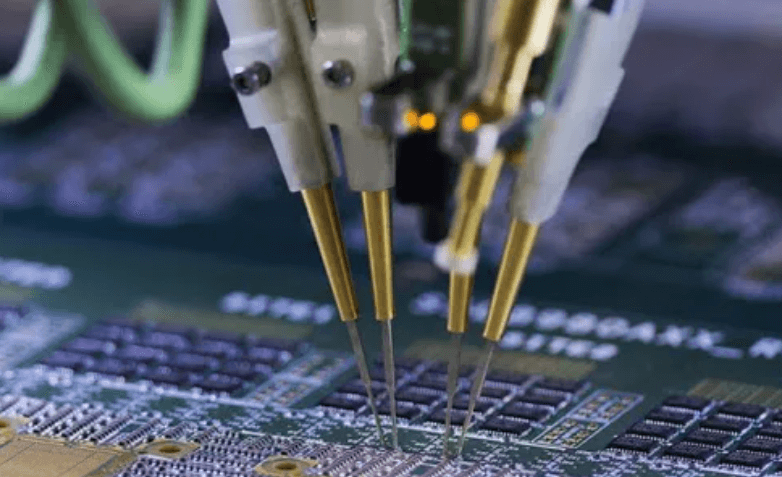
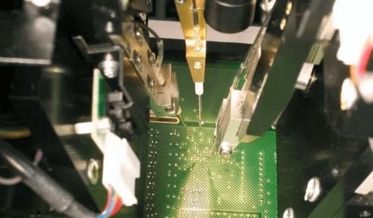
Flying Probe Testing
Flying probe test can check the short circuit, open circuit and component values, using four probes to high voltage circuit board insulation resistance and low conduction test, and do not need to do the test fixture, run the test program can be directly PCB test is extremely convenient, save test cost, minus the manufacture to the test time, improve the efficiency of the shipment, suitable for testing small batch and sample.