
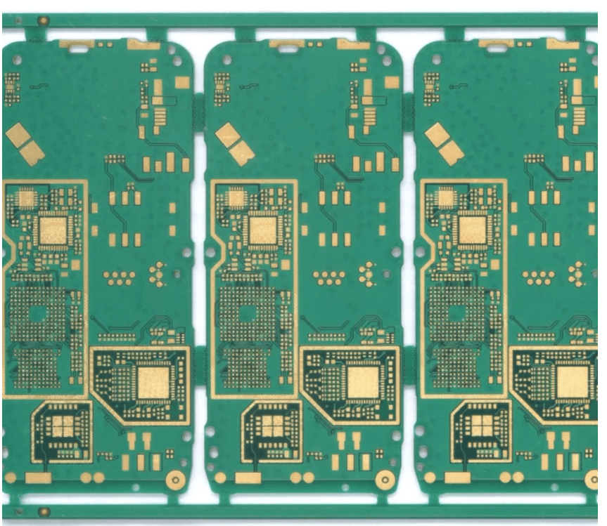
To improve PCBA production efficiency, reduce production costs, usually the PCB circuit boards will be panelized for board assembly production, which can facilitate the PCBA soldering, but also save time.
The purpose of the PCB Panelization?
Improve the efficiency of SMT assembly.
The more the number of boards contained in a panel, the less the average time of a single PCB in the track transmission operation, the higher the utilization rate of mounting equipment, which can greatly improve the efficiency of SMT production.
Improve SMT production quality.
Prevent adverse problems in the SMT production process. After the PCB is panelized, additional edges are added, which can prevent the components on the edge of the PCB board from being damaged during the SMT process and improve the production quality of the overall SMT.
Easy to operate and save time.
Multiple PCBs are assembled in one panel, which is not only easy to operate but also greatly saves production time.
PCB Panelization Guidelines
1. Normally the width of PCB panel ≤is 260mm, or ≤300mm
2. It’s better for fabrication to make the shape of the PCB panel close to square or rectangle.
3. Try to design the border of the PCB panel with a closed loop to ensure that the PCB panel will not deform when SMT assembly.
4. The center distance between each board control between 75mm-145mm.
5. The components and PCB board edge should leave more than 0.5mm space, to ensure the normal operation of the cutting tool.
6. There should be added positioning holes on the four corners of the panel edges, hole size can be 4mm±0.01mm, and pay attention to the high accuracy of aperture and position, smooth hole wall without burr.
7. No wiring or soldering is allowed within 1mm of the edge positioning hole.
8. The fiducial marks should be added when making PCB panelization, which is generally located at the diagonal of the panel edge.
9. Usually, there should create a solder mask opening area 1.5mm larger than the reference point should be set aside around the fiducial marks.
Common Types of PCB Panelization:
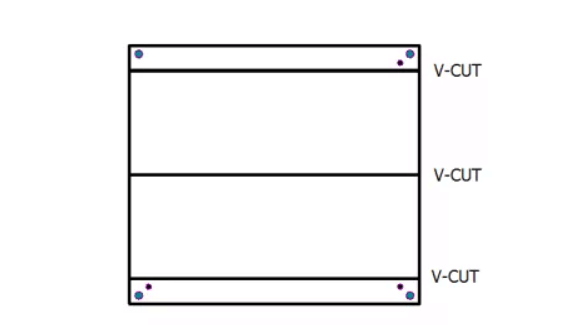
1. V-CUT(V-Scoring)
The main purpose of designing V-Scoring is to facilitate operators in board Scoring after PCB board assembly. A scoring machine is generally used in PCBA board Scoring so that we can easily separate boards and remove board edges.
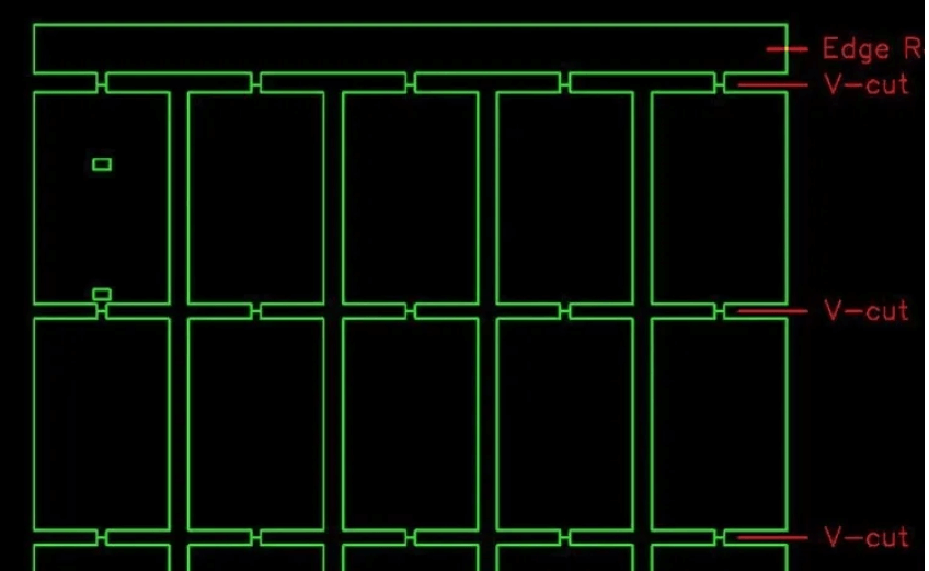
2. Routing:
Routing refers to between the board and the board or inside the board as required to mill empty by the milling machine, equivalent to cut out. This connection is more used in the board with the half holes assembly, using a very narrow plate for connection. There is a disadvantage for routing: after separating the boards, there will be a very obvious convex point.

3. Stamp hole
The stamp is to use a very small hole between the PCBs, looks like the serrated on the stamp, so-called stamp hole connected. The stamp hole is between the board and the board all around the need for high control burr, that is, can only use a little stamp hole instead of V-cut lines.
To meet the requirements of the production process, in the PCB panel, the length of the connecting tab is generally 4-6mm, the size of the non-metallic holes is generally 0.3mm to 0.5mm, and the spacing between the holes is 0.8-1.2mm.