
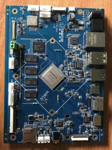
PCBs consist of different numbers of layers ranging from single to multiple layers. Several layers determine the power and functionality of PCB. These layers help carry power that applies to many home appliances, e.g., kitchen appliances, smart watches, mobile phones, medical devices, aerospace, storage devices, etc. You may count PCB layers number by using via-hole technology. In single-layer PCBs, you can easily see only one layer is present. However, a punch hole is necessary to see layers in multilayer PCBs.
PCB layers are like lasagna and consist of dielectric and conductive materials. The following factors usually decide the numbers of any PCB.
1. Applications of PCB:
You have to decide for which purpose you want to design PCB. Only some single-layer PCBs are suitable for complex and multifunctional devices. You must go for multilayer PCBs for high quality, speed, and more meaningful projects.
2. Budget:
Your budget will also decide whether you go for single-layer PCB, double-layer PCB, or multilayer PCB. High-capacity projects demand multiple-layer PCBs that are more costly.
3. Operation frequency:
Operation capacity should be considered in your mind when choosing PCBs. For high speed and power, you must select a multilayer PCB.
4. Time lead:
Time lead is also an essential factor to be considered when you choose many PCB layers. To order bulk, you must go for a single-layer or double-layer PCB. The estimated lead time for single-layer PCBs is 14 days, and for multilayer PCBs, more than 20 days. The cost will also reduce the lead time.
5. Requirement of signal layer:
Siga layers are also crucial in designing PCBs. Signal layers have a strong correlation with pin density. As the layers go up, pin density will reduce. For example, for 1.0 pin density, signal layers will be 2, and for 0.2 pin density, layers will go up to 14 in number.
Layers of PCBs:
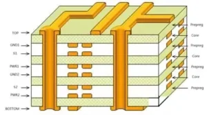
Single-layer PCBs only have one layer, but multilayer PCBs have different layers ranging from four to twelve. We can take a multilayer PCB structure like a sandwich in which dielectric and conductive materials stack together.
Arrangements of layers may affect electromagnetic compatibility. For example, evenly distributed layers of PCB will show undesirable effects because they are in a symmetrical position from the core of the PCB. To get desirable electromagnetic compatibility, layers should be placed close to the center of the PCB. To increase signal transmission, layers should also stack together as closely as possible.
Steps to determine the number of PCB layers:
You can determine the number of layers by using the three simple steps below;
1. Choosing the number of layers:
Single or double-layer PCB:
Single-layer PCB is simple in structure and only consists of one layer of conductive dielectric covered with copper and solder mask. More over, Single-layer PCB represents three colors green for the solder mask, brown for copper, and gray for the dielectric.
Single-layer PCBs are easy to manufacture, so that you can order in bulk. These are affordable and uncomplicated, so they are efficiently repaired. Single-layer PCBs have been used for several decades; however, most home appliances and industries have been replaced with multiple-layer PCBs. Single-layer PCBs still operate in many electrical devices, e.g., radio calculators, LED lights, printers, cameras, coffee makers, etc.
Double-layer PCBs have more advanced technology. Double-layer PCB is the same as single-layer PCB but has high capacity and much better performance than single-layer PCB. It is the most widely used option in today’s market due to its low cost and better performance. Double-layer PCB is much like single-layer PCB but has a thick dielectric cover with copper on both the top and bottom sides.
Besides, double-layer PCB represents a sandwich of thick grey dielectric layers lying in the middle, the brown color represents copper on both top and bottom sides, and the light green represents the solder mask on both sides. Double-layer PCBs are more flexible and denser, which makes them more favorable to use in electrical appliances. What else, double-layer PCBs are also cost-effective and straightforward to design, making them easy to repair. Double-layer PCBs applies to many devices, e.g. printers, LEDs, amplifiers, etc.
It would help if you chose single or double-layer PCBs for simple devices at home but avoid them for interfaces with controlled impedance. Single or double-layer PCBs are not recommended for DVDs, USBs, etc.
Four-layer PCB:
Four-layer PCB is different from single and double-layer PCB. Then, four-layer PCB is more complex as it has separate copper and conductive material layers. Four-layer PCB consists of four copper strips and three dielectrics with top and bottom solder masks. Then, Four-layer PCB represents nine strips with brown, green, and grey colors. Four-layer PCB is more durable, flexible, light weighted, and compact. Four-layer PCBs use in satellites, X-rays, CAT scan technology, nuclear technology, and space equipment. These are more complex, and experts are required to handle these PCBs.
Four-layer PCB is much better than single or double-layer PCB because it is not costly and performance is also better. 4-layer PCB recommends in case of simple circuits but avoids use in CPU boards.
Six-layer PCB:
Six-layer PCB is the same as a four-layer PCB in structure with two extra copper and dielectric layers. It has the second and fourth layers as a dielectric and the first, third, and fifth as prepregs. In a six-layer PCB, two layers are planes, and the others are signals. These are thicker, high-capacity, compact in size, and more powerful. Six-layer PCBs are high quality and recommended to use in most motherboards. They also apply to computers, fire alarms, GPS technology, etc.
Multilayer PCB:
Multilayer PCBs are comprised of more than two layers and depend on the budget and complexity of the project you want. And then, multilayer PCBs may consist of two-layer, four, ten, or twelve layers.
10-layer PCB usually fits into a 1mm socket, equal to 8-layer PCB but better in performance than eight layers PCB. 10-layer PCB is suitable for use in SODIMM computers. 12-layer PCBs are also available in the market that is used in heavy industries.
2. design a layout:
You can start with the top and bottom layers of the PCB. What’s more, You can add two between the top and bottom layers if you want to add more layers. You can redesign the layout and fit everything into this, one top, one bottom, and two inner layers. PCB layers can be determined with different factors, including PCB technology, PCB stack-ups, Vias, placements of components, and many features. If you want to add more connections, you can add them according to your demand.
3. Layer distribution of PCB:
Following determining the necessary number of layers, the ensuing tasks must be carefully carried out to arrange all circuits sensibly. Two important factors should be followed,
- Distribution of ground and power layer
- Signal layer distribution
There are different options for distributing layers in PCB. 4 layers stack often uses signals/GND/Power/Signal, and six layers stack ordering is Signal/GND/Power or Mixed with signals/GND/Signals. GND often prefers the second layer providing a shield from high-speed signals.
As the number of layers increases, there may be more configuration options for the ground, power, and special signal layers. However, there are several guidelines to follow while creating these layer arrangements:
- The power layer should be next to the particular signal layer, and the copper power layer should serve as a shield.
- A ground layer can be placed between two signal layers to avoid direct contact.
- Power layers and Multiple ground can effectively reduce impedance.
- The symmetrical structure of layers
How many layers can be used depends on the application’s functional requirements and economics. Pin density will be defined later; it is critical in determining the number of layers in printed circuit boards (PCB).
The printed circuit board (PCB) wiring density must be determined using appropriate tools. It is also necessary to decide what signals will be transmitted through this, and then specific wiring requirements, such as differential lines, sharp signal lines, and so on, will be considered.