
PCB Prototyping is the process of making a circuit in the form of a printed circuit board. This printed circuit board makes connecting your components more secure and robust. A PCB prototype is better than a breadboard with wired components. This method is especially true when presenting your projects. You can prototype a PCB manually or seek a reliable PCB manufacturer. Usually, a manufacturer produces better and longer-lasting PCBs.
There are several processes involved in prototyping a PCB. This article will outline these processes to make your PCB prototyping faster and easier.
Decide on a PCB Layout Software
Today, several PCB layout software can help you design your PCB prototype. There are both paid and free software. There are also web-based PCB design tools. Whatever tool you choose, what’s important is that you are comfortable using it, and it meets your design requirements. You can research the capabilities of several PCB Design tools listed below.
Here are examples of free PCB layout software that you can download and install on your PC.
- Libre PCB
- KiCAD
- Express PCB
- Design Spark PCB
Here are examples of paid PCB layout software. Usually, medium to large-sized companies use these kinds of software. You can download a free trial of the software before paying for it.
- Altium Designer
- Allegro PCB Designer
- OrCAD
- Autodesk Fusion 360
- Circuit Studio
- PADS PCB Design
Here are examples of cloud-based PCB layout software. With this, you don’t have to install a large chunk of software on your PC. Sometimes, downloading software components is optional.
- EasyEDA
- ai
- CADLab
- Altium 365
- Solidworks PCB
Note that your PCB layout software should generate fabrication or manufacturing outputs so you can send these outputs to your PCB manufacturer. After that, your PCB manufacturer should send you a finished PCB ready for prototyping. You can also do a prototype PCB assembly with components stuffed on your boards. With this method, you don’t have to solder components manually on your PCB. This process can save you time on your projects. However, note that PCB assembly has some overhead setup fees.
Make a Clear Schematic Diagram
What’s the purpose of a Schematic?
You must make a PCB prototype with a clear schematic diagram. A schematic diagram represents the wirings of all the components on your PCB. Usually, the diagram starts from a circuit designer’s idea. After that, he lays it out on an editor program. The designer can revise the schematic diagram repeatedly. This process can continue until he thoroughly debugs the final circuit.
How to Make a Schematic?
Fortunately, making a schematic is easy, especially with the available EDA tools today. Usually, a schematic editor is already part of an EDA’s IDE (Integrated Development Environment). The editor usually works with the PCB layout, parts footprint library, and parts symbol library editor. Several schematic editors simply drag and drop part symbols into their editing window, ready to be wired by the user.
Check your Components if they are available in your Parts Library.
You may discover you have components that need to be added to your parts library while making your schematic. This process is nothing to be alarmed about; you may treat this as a timely learning experience. You can browse several component manufacturers’ websites and see if you can download that missing part’s CAD library. You can also visit trusted third-party CAD library websites and find your missing component.
Examples of Third-Party CAD library websites
- Ultra Librarian
- SnapEDA
- SamacSys
You can create your part if you cannot find your missing component in any of the abovementioned processes. This process entails going through your PCB design software’s symbol and footprint editor. Browse your software’s manual or help menu to learn how to use these editors.
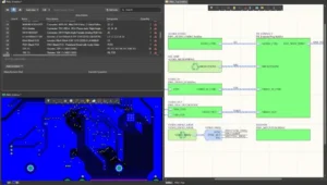
Create or Route your PCB using a PCB Layout Editor.
A PCB layout editor will help you layout your PCB according to your intended design. The PCB layout editor and the schematic editor usually work hand-in-hand to complete the design task. Several EDA tools today have a decent PCB layout editor to complete most PCB designs.
What are some Characteristics of a PCB Layout Editor?
- It may have auto-routing capabilities. Auto-routing means you’ll let the computer do the routing of tracks for you. Some can do auto-placement of components, too.
- Has DRC (Design Rule Checking). Design rule checking is a critical feature of any PCB layout editor. DRC will check your design for placement, track, or other design issues before they reach manufacturing.
- Can sync or update any component or wiring modification with the schematic editor. This feature is sought after by many PCB designers.
- It may help you wire tracks of equal length. This method is an important feature, especially if you’re wiring high-speed tracks that require impedance matching.
You should be able to create fabrication outputs after finishing your design and doing DRC checks.
Create Fabrication Outputs
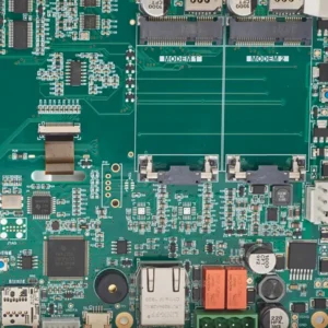
You’ll usually create fabrication or manufacturing outputs after creating your PCB design. This process is true if you want your boards fabricated by a PCB manufacturer. With this, you must check how to generate fabrication outputs on your PCB design software. There is usually a menu for this.
Fabrication outputs or data are usually in Gerber format. These Gerber files are formatted to work well with PCB fabrication machines. Check your Gerber output parameters with your PCB manufacturer before generating them.
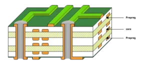
Usually, you’ll have to familiarize yourself with layer information about your Gerbers. Such layers as:
- Top and Bottom Tracks layers.
- Top and Bottom SilkScreen layers.
- Inner layer tracks (if any).
- Solder Mask and Solder Paste layers.
- PCB OUtline layer.
- Fabrication or Assembly layer.
Also, remember to output your drill data (DRL) file. This file is essential, especially if your design has drill holes.
Create Assembly Outputs
This process is necessary if you want your PCB already assembled with components. You may want PCB assembly, especially if you have several boards that are time-consuming to produce. You may also want this process if you have difficulty soldering specific components.
There should be an option in your PCB design software for outputting assembly files. The assembly files are usually composed of the following:
- Position file.
- BOM file.
The position files, also called pick & place files or centroid files, define the X & Y position of all the components in your PCB. This info is necessary for a pick-and-place machine to correctly place your components on your board. The BOM files contain important information regarding each component, such as reference designator, manufacturer part number, PCB footprint, and description.
Check your Fabrication Outputs with a Gerber Viewer
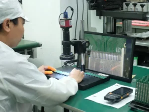
You can use a Gerber viewer to check if you have no more issues in your final design. It can be that you need to catch certain hard-to-spot elements. Such things include missed solder paste pads, masks, silkscreen references, tails on your copper tracks, and the like. A good Gerber Viewer can zoom in and out to get a total view of your design.
Some PCB design software already has a Gerber viewer integrated into their system—such as KiCAD (using Gerber Viewer) or Altium Designer. If your software has none, don’t worry; plenty of third-party Gerber viewers are available. Below are examples of them.
- Gerbv
- ViewMate
- Zofz PCB Viewer
- Gerber Viewer
Prepare to Send your Manufacturing Data to your PCB Manufacturer
Your PCB manufacturing data should be secure when you send it to your PCB manufacturer. Usually, they must be placed in one zip file so they don’t get scattered around. After this, ensure proper communication with your manufacturer regarding manufacturing your boards.
You may discuss your boards’ proper materials and processes with your manufacturer. Some things to consider are:
- What is the thickness of your board, and how many layers?
- What is the PCB material you want?
- What is the pad finish you want?
- What is the color of your silk screen?
- Do you need lead-free boards?
- In assembly, do you need a stencil?
- What kind of testing do you want your fabricator to do to your boards when they finish making them?
Finally, agree on payment and delivery terms.
It would help if you continue communicating with your manufacturer until they have finalized your board. Please don’t close your communication lines with them. It can be that your design has flaws related to their manufacturing processes. The longer these flaws are not corrected, the longer your design’s lead time will be.
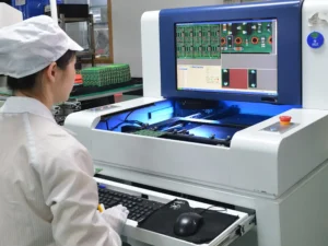
Receive your PCB Prototype and Inspect them.
Hopefully, you’ll receive your PCB prototypes in time. Check and inspect them upon receiving them to verify if any issues exist. Your manufacturer should be open to discussing these kinds of things, and it should be part of their customer support system. With this, finding reliable PCB manufacturers that provide after-sales support is vital.
Finalize your PCB Prototype
Debug your PCB prototype and finalize it to make your project presentation. If needed, you may do another revision of your board. This process is called re-spin. A good and thought-after design usually has few (or even no) re-spins. In this case, you can save budget for your next project idea.