
As soon as you understand exactly what you want from the pcb prototypes and have accumulated the required information, you can start the pcb prototyping procedure. A seasoned PCB business may give you support during this procedure. Pick a business which provides responsive customer support and useful tools to make the process go as smoothly as you can.
Working with us, UETPCB offers complete turnkey solutions might help simplify the procedure, because you avoid needing to communicate with numerous businesses.
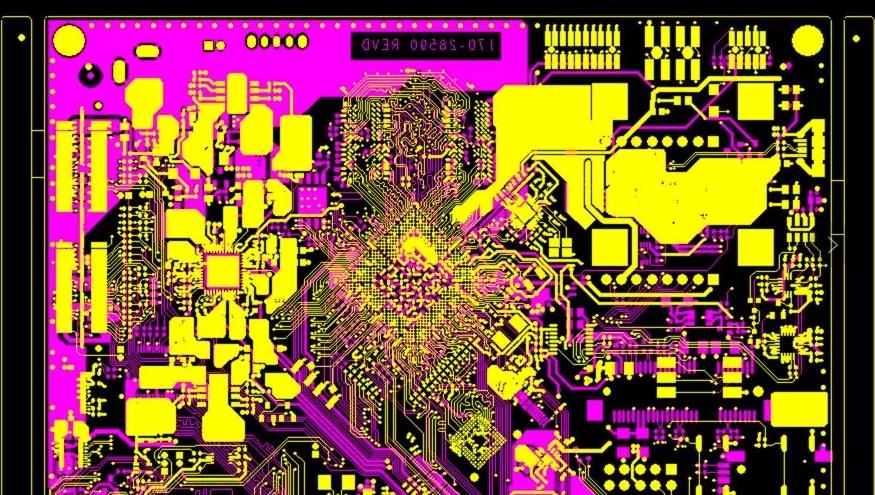
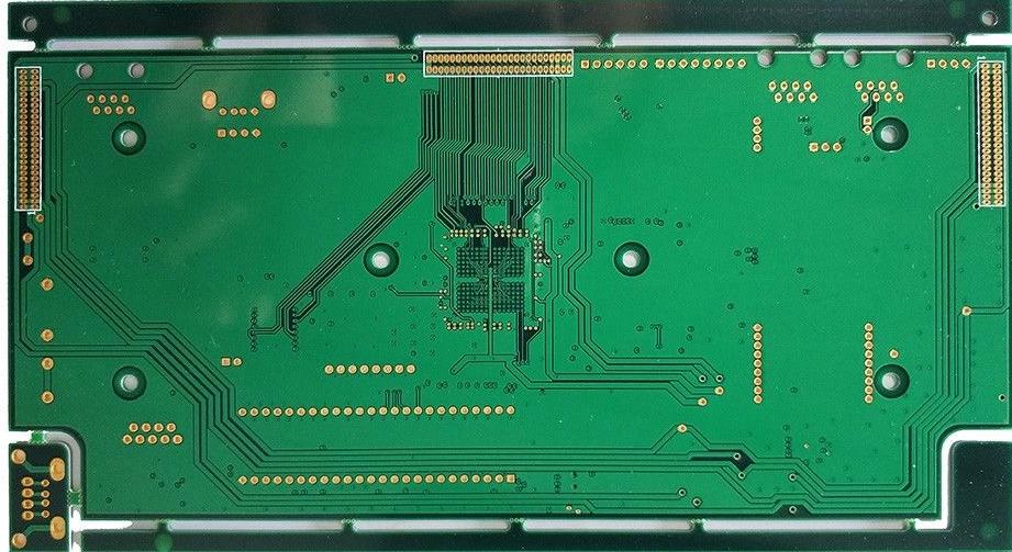
PCB Design/Layout Process Steps
1. Layout
The very first step in producing a PCB prototype is designing. As stated previously, you can use one of numerous PCB design software suites to make your layout.
2. Schematic
The design describes crucial advice that engineers and manufacturers will utilize during the manufacturing procedure. It features information concerning the materials, hardware and components utilized in production and decides the board’s purpose, its own attributes and the positioning of components. Some significant facets of this stage are choosing the ideal panel dimensions and grid.
This design is a portion of the first design stage. When designer completes the initial assessing, they will conduct a preliminary check for possible flaws and fix any that appear. You may then run simulations utilizing a technical PCB layout tool to guarantee the board to function correctly and it functions as a more comprehensive layout test. The designer then converts the digital design into what’s called a netlist, which explains the interconnectivity of these included elements.
It is necessary to conduct design rule checks frequently during the design process. This strategy allows you to resolve problems and enables a more efficient design procedure.
3. BOM
Next a BOM (Bill of Materials) is needed. This is a listing of all of the components and materials you require for creation and information about them. If you’re relying upon a producer to supply your components, this really is the record they’ll utilize to make sure they get the proper ones.
The BOM includes critical information for every component, such as:
(1)Quantity: The quantity of components required.
(2)Reference Designators: Codes used to identify human pieces.
(3)Values: The specifications for each component described in the right units, like ohms or farads.
(4)Footprint: The positioning of every part on the PCB board.
(5)Manufacturer Number: The complete component descriptions of manufacturer part number should be clear.
After the BOM and schematic have been completed, a design engineer and part engineer will assess the record and collect the vital pieces. The part engineer is responsible for picking components which will function for the layout and fit within the price and size requirements of the customer.
4. Routing
You must then design the navigation, by means of hints, you may use to join each component of this PCB. Different factors play a part in preparing routing, such as electricity levels, signal-noise production and sound sensitivity.
Many PCB design software applications utilize the netlist you have already developed to program on the routing. A number of these apps can automatically figure out the best paths depending on the amount of accessible layers and other aspects. This procedure sometimes takes some time — particularly for bigger circuit boards or planks with a great deal of components.
5. Checks
You need to check your layout regularly during the procedure for virtually any performance problems, but until you proceed in the manufacturing stage, do you last comprehensive examination to appraise each component of your layout for possible issues.
Common issues to watch out for include thermal problems like heating stains. Your layout should keep the plank one constant temperature. Some design features like the existence of thermal avenues, varying aluminum thicknesses, a sizable PCB size and the amount of PCB prototype layers may give rise to heat stains and temperatures that are inconsistent.
Along with some thermal check, you need to run a design rule check, a layout-versus-schematic (LVS) test, an electrical rule checks (ERC) and an antenna test. Many producers also perform other evaluations for extra excellent assurance.
After finishing your tests, you could send your layouts to some PCB manufacturers for the PCB fabrication, at same time you should consider their capabilities if meet with your requirements.
PCB Prototype Services
Before you purchase a complete run of printed circuit boards to your job, you want to be certain that your layout works flawlessly. To do this economically and cost-effectively, you will need to create a pcb prototype of your board — a little streak of your layout to check its performance.
However, you don’t need to waste time on pcb prototyping process. That is why you have to work using a PCB manufacturing firm like UETPCB that may help you get precise, cost-effective pcb prototypes fast. As soon as you’re happy with your pcb prototypes, we can even finish your entire production run using the exact same dedication to quality and efficacy.
Another means to assist your pcb prototyping process go smoothly is to be certain to know what it involves so you understand what to expect and can easily supply the essential info. So, what precisely does pcb prototyping involve?
Advantages of PCB Prototyping
We advise that you produce a pcb prototype prior to purchasing a complete production run of a new PCB prototype layout. We ensure our prototype PCB support is user-friendly and fast so that you may examine your board without hassle or delay. Here Is What pcb prototyping Allows You to perform:
(1)Detect design defects early in the manufacturing process before you spend significant capital
(2)Cost-effectively test multiple layouts
(3)Get a true portrayal of how your board will operate
Ahead PCB Prototyping
Before beginning the PCB prototyping procedure, be certain pcbprototyping is ideal for your requirements. Although it’s beneficial for many jobs, it is not essential for every single kind. In case you choose to make a pcb prototype, you’re going to want some simple details regarding your job to begin.
Deciding If You Require a pcb Prototype: Prototypes are best for when you wish to check your layout or execute an excellent check of your PCB.
You ought to use a prototype whenever you use a factory for a new job. If you have already successfully produced a digital product with that board, then you might not require a pcb prototype. Should you create any design modifications or produce a totally new PCB prototype or merchandise, nevertheless, you need to purchase a pcb prototype.
For our rapid PCB prototyping service, we could meet orders of 5 to 100 units and extend a construct time of four to five business days.
Organizing for your PCB Prototyping Process
To submit your design for pcb prototyping or to get a quote for PCB prototype design solutions, you ought to prepare some info regarding your design. Generally, more information is much better — this can allow you to get the results you desire. Following is some information you need to include when submit your design to manufacturer:
(1)the number of layers
(2)Board Thickness
(3)Board Dimension
(4)Copper thickness
(5)Minimum trace width/space
(6)Minimum hole sizes
(7)Minimum annular ring
(8)Surface Finish
(9)Solder mask color
(11)Silkscreen color
(12)Drill file with NC data
(13)Drill file application listing
You may submit your layout files utilizing various software titles. We’ll convert the document to Gerber RS-274X, that’s the perfect file type.
Our PCB Prototype Capabilities
Though it may look more effective to jump into a complete production run, beginning with a pcb prototype is likely to make your manufacturing process more efficient and cost-effective in the future and result in enhanced quality and more predictable performance.
If you utilize UETPCB, you minimize the additional time necessary to generate a pcb prototype, while maximizing quality and precision. We can mimic your design in only three to seven days. We help you keep down costs by enabling prototype orders as little as five bits. For sure, we can help you save cost of development by finding design errors and other problems early before manufacturing procedure.
We also save time and money because we provide all parts of PCB prototyping, from manufacturing to part sourcing to meeting. This one-stop-shop approach means that you don’t need to hunt about for a different firm for every area of the procedure.
In UETPCB, we’ve got an in-house excellent control section and fulfill all of the demands of ISO9001:2008, the benchmark for quality control systems. Our pcb prototype manufacturing tolerances supply you with a precise indicator of the way the board will function in real life ailments.