
Basic knowledge of PCB
Before defining pcb manufacturing process,it will be useful to learn about pcb and it’s structure. The printed circuit board (PCB) is the foundation in most electronics products – both as a physical support piece and as a wiring area for surface mount and socket components. PCBs are most commonly made of fiberglass, composite epoxy, or another composite materials.
The PCB mainly contains the following parts:
- Pad: A metal hole used for soldering component pins.
- Via: A metal hole used to connect the pins of components between layers.
- Mounting hole: used to fix the printed circuit board.
- Wire: The copper film of the electrical network used to connect the pins of the components.
- Connectors: components used to connect between circuit boards.
- Filling: Copper coating for ground wire network, which can effectively reduce impedance.
- Electrical boundary: used to determine the size of the circuit board, all components on the circuit board cannot exceed the boundary.
There are three types of PCB structure:
-
Single-Layer PCB:
- There are copper foil wires on only one side of the circuit board, and no copper foil wires on the other side. The circuit of early electronic products was simple. Only need one side to connection and conduction, and could place the path on the other side without copper foil.
-
Double-Layer PCB:
- There are copper foil wires on both sides of the circuit board. And the paths of the front and the back can connect to each other through vias. Since both sides can be wired, the usable area is twice that of a single panel, which is more suitable for products with complex circuits. In the design, the parts are placed on the front side, while the back side is the welding surface of the part feet.
-
Multi-Layer PCB:
- Usually by using multiple etched double-sided boards to make Multi-Layer PCB. Stacking an insulating layer (Prepreg) between the boards and laying copper foil on both sides of the outermost layer and then pressing them together. Since use multiple double-sided panels to press, the number of layers is usually an even number. The copper foil layer pressed inside can be a conductive layer, a signal layer, a power layer or a ground layer. In theory, the multilayer board can reach more than 50 layers, but the practical application area is currently about 30 layers.
PCB are very versatile. Most electronic products have printed circuit boards, from computer components (keyboards, mice, motherboards, optical drives, hard disks, graphics cards), to LCD screens, TVs, mobile phones, and telephone, electronic watch, digital camera, satellite navigation, PDA…) are almost a part of life.
The working principle of PCB:
A very basic type of printed circuit board is a flat, rigid insulating material with a thin conductive structures adhered to one side. These conductive structures produce geometric patterns consisting of rectangles, circles, and squares. Use long and thin rectangles as interconnections (that’s the equivalent to wires), and use various shapes as connection points for components.
The future development of PCB:
With the rapid development of the computer, communication equipment, consumer electronics and automobile industries. The PCB industry has also achieved rapid development. With the development of printed circuit products, the requirements for new materials, new technologies and new equipment are getting higher and higher. In the future, the printed electrical material industry should pay more attention to improving performance and quality while expanding its output; the printed circuit special equipment industry is no longer a low-level imitation, but to the development of production automation, precision, multi-function, and modern equipment.. The PCB production integrates the world’s high-tech technologies. The printed circuit production technology will adopt new technologies such as liquid photosensitive imaging, direct electroplating, pulse electroplating, and multilayer boards.
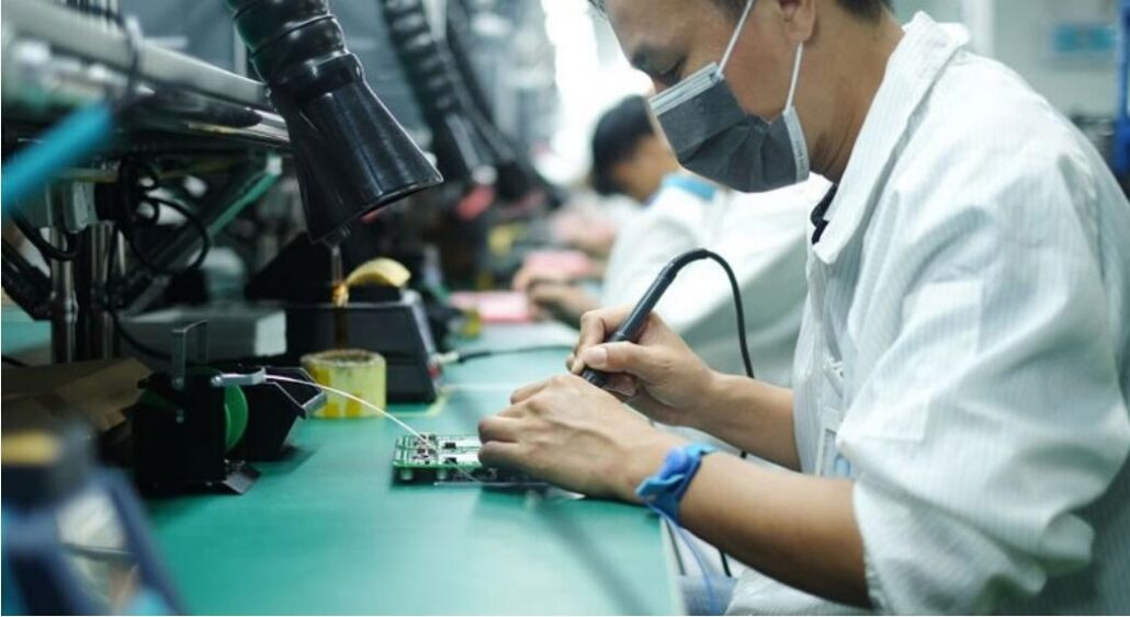
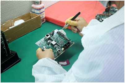
The PCB Manufacturing Process
Closer to home, now let’s take a look at the PCB production process.
The production of PCB is very complicated. Taking a four-layer printed board as an example. The production process mainly includes PCB layout, core board production, inner PCB layout transfer, core board punching and inspection, lamination. Drilling and hole wall Copper chemical precipitation, outer PCB layout transfer, outer PCB etching and other steps.
1. PCB layout
The first step in PCB production is to organize and check the PCB layout. The PCB production factory receives the CAD files from the PCB design company. Since each CAD software has its own unique file format. The PCB factory will convert it into a unified format-Extended Gerber RS-274X or Gerber X2. Then the factory engineer will check whether the PCB layout conforms to the manufacturing process. And whether there are any defects and other issues.
2. Production of core board
Clean the copper clad laminate. If there is dust, it may cause the final circuit to be short-circuited or broken. An 8-layer PCB is actually made up of 3 copper clad laminates (core boards) plus 2 copper films, and then glued together with prepregs. The production sequence is to start with the middle core board (4 and 5 layers of circuits), continuously stack together, and then fix. The production of 4-layer PCB is similar, except that only use one core board and two copper films.
3. Inner PCB layout transfer
First, make the two-layer circuit of the middle core board. After cleaning the copper clad laminate ,a photosensitive film will cover on the surface. This film will solidify when exposed to light. Form a protective film on the copper foil of the copper clad laminate. The two-layer PCB layout film and the double-layer copper clad laminate then inserted into the upper PCB layout film to ensure the stacking position of the upper and lower PCB layout films.
The photosensitive machine irradiates the photosensitive film on the copper foil with a UV lamp. The photosensitive film is cured under the light-transmitting film, and there is still no cured photosensitive film under the opaque film. The copper foil covered under the cured photosensitive film is the required PCB layout circuit, which is equivalent to the function of the laser printer ink of the manual PCB. Then use lye to clean the uncured photosensitive film. And the required copper foil circuit will be covered by the cured photosensitive film. Then use a strong alkali, such as NaOH, to etch away the unnecessary copper foil.
4. Core board punching and inspection
Successfully produced the core board. Then punch alignment holes on the core board to facilitate alignment with other materials. Once press the core board together with other layers of PCB, it cannot be modified, so inspection is very important. The machine will automatically compare with the PCB layout drawing to check for errors.
5. Laminating
A new raw material is needed here, called a prepreg. It is the adhesive between the core board and the core board (PCB layers>4). As well as the core board and the outer copper foil, which also plays a role in insulation. To fix the lower copper foil and the two layers of prepreg in advance. Through the alignment hole and the lower iron plate, and then place the finished core board in the alignment hole. And finally the two layers of prepreg, a layer of copper foil and A layer of pressure-bearing aluminum plate covers the core plate.
Place the PCB board clamped by the iron plate on the support. And then sent to the vacuum heat press for laminating. The high temperature in the vacuum hot press can melt the epoxy resin in the prepreg and fix the core boards and copper foils together under pressure. After completing the lamination , remove the upper iron plate that presses the PCB. Then remove the pressure-bearing aluminum plate. The aluminum plate also has the responsibility of isolating different PCBs and ensuring the smoothness of the outer copper foil of the PCB. Both sides of the PCB taken out at this time, a layer of smooth copper foil will cover the PCB .
6. Drilling
To connect 4 layers of non-contact copper foils in the PCB, first drill through the through holes to open the PCB, and then metalize the hole walls to conduct electricity. Use the X-ray drilling machine to locate the inner core board. The machine will automatically find and locate the hole on the core board. And then punch the positioning hole on the PCB to ensure that the next hole is drilled from the center of the hole. Put a layer of aluminum plate on the punching machine machine, and then put the PCB on it.
In order to improve efficiency, according to the number of PCB layers, stacking 1 to 3 identical PCB boards together for perforation. Finally, cover the uppermost PCB with a layer of aluminum plate. Use the upper and lower layers of aluminum plate to prevent the copper foil on the PCB from tearing when the drill bit drills in and out. In the previous lamination process, the molten epoxy was squeezed out of the PCB, so needs to cut it off. The profiling milling machine cuts its periphery according to the correct XY coordinates of the PCB.
7. Copper chemical precipitation on the hole wall
Since almost all PCB designs use perforations to connect different layers of lines. A good connection requires a 25-micron copper film on the hole wall. The thickness of the copper film needs to complete by electroplating. But the hole wall is composed of non-conductive epoxy resin and glass fiber board. So the first step is to deposit a layer of conductive material on the hole wall. And form a 1 micron copper film on the entire PCB surface by chemical deposition, including the hole wall. Use the machine to controll the entire process such as chemical treatment and cleaning.
8. Outer PCB layout transfer
Next, the PCB layout of the outer layer will transfer to the copper foil. The process is similar to the previous transfer principle of the inner core board PCB layout. The PCB layout transfer to the copper foil by photocopying film and photosensitive film. The only difference is will use positive films as the board.The internal PCB layout transfer uses the subtractive method, and use the negative film as the board. Cover the PCB with a cured photosensitive film as a circuit, and clean the uncured photosensitive film. After etching the exposed copper foil ,the cured photosensitive film will protect the PCB layout circuit.The transfer of the outer PCB layout adopts the normal method, and use the positive film as the board.The cured photosensitive film cover the non-circuit area on the PCB.
After cleaning the uncured photosensitive film, electroplating is performed. Do not electroplate where there is a film. And where there is no film, copper plateing first and then tin plating. After removing the film, alkaline etching is performed, and finally the tin is removed. The circuit pattern remains on the board because it is protected by tin. Clamp the PCB with clamps, and electroplate the copper. As mentioned earlier, in order to ensure that the holes have sufficient conductivity, the copper film plated on the hole walls must have a thickness of 25 microns. So the computer will automatically controll the entire system to ensure its accuracy.
9. Outer PCB etching
Next, a complete automated assembly line completes the etching process. First, clean the cured photosensitive film on the PCB. Then use a strong alkali to clean the unnecessary copper foil covered by it. Then use the tin stripping solution to strip the tin plating on the PCB layout copper foil. After cleaning, the 4-layer PCB layout is complete.The production process of PCB is more complicated, and it involves a wide range of processes. From simple mechanical processing to complex mechanical processing, common chemical reactions, photochemical, electrochemical, thermochemical and other processes, computer-aided design CAM. And many other aspects of knowledge.
Moreover, there are many process problems in the production process and will encounter some new problems from time to time. Some of the problems disappear without finding out the cause. The production process is a non-continuous assembly line form. So any problem in any link will cause the entire line to stop production and the consequences of mass scrapping.