
16 requirements of SMT process for component layout design
The layout of components should be designed according to SMT electronic processing equipment and process characteristics and requirements. Different processes, such as reflow soldering and wave soldering, have different layouts for components. When double-side reflow soldering, there are different requirements for the layout of side A and side B. Selective wave soldering and traditional wave soldering also have different requirements.
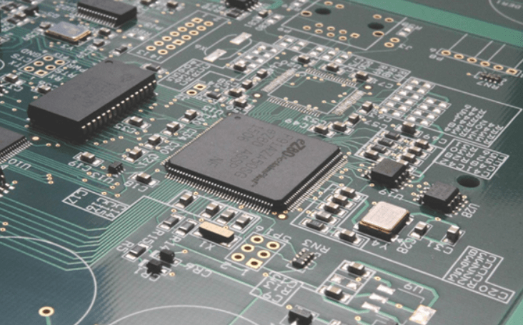
The basic requirements of SMT process for component layout design are as follows :
1:The distribution of components on the printed circuit board should be as even as possible. The heat capacity of high-quality components during reflow soldering is large, and the concentration is easy to cause local low temperature and lead to virtual soldering. At the same time, the uniform layout is also conducive to the balance of gravity center, in the vibration and impact experiment, it is not easy to appear components, metallized hole and welding plate destroyed phenomenon.
2: Components should be arranged in the same direction on the printed circuit board. Similar components should be arranged in the same direction as far as possible. The characteristic direction should be consistent to facilitate the assembly, soldering and testing of components. For example, the positive of electrolytic capacitor, the positive of diode, the single pin end of triode and the first pin of integrated circuit are arranged in the same direction as possible. The printing orientation of all component Numbers is the same.
3: The size of the heating head of the SMD repair equipment can be operated should be set aside around the large components.
4: Heating components should be kept as far as possible away from other components, generally placed in the corner, the chassis ventilation position. The heating components shall be supported by other leads or other supports (such as adding heat sink) to keep a certain distance between the heating components and the surface of printed circuit board. The minimum distance shall be 2mm.The heating components is connected with the printed circuit board in the multilayer board.
5: Temperature sensitive components should be kept away from heating components. Such as transistors, integrated circuits, electrolytic capacitors and some plastic shell components, etc., should be as far away from the bridge reactor, high-power components, radiators and high-power resistors.
6: The layout of the components and parts that need to be adjusted or changed frequently, such as potentiometer, adjustable inductance coil, variable capacitor micro switch, safety tube, key, plug and plug, etc., should take into account the structural requirements of the whole machine and place them in a position that is convenient for adjustment and replacement. If the machine adjustment, should be placed on the printed circuit board easy to adjust the place; If the adjustment outside the machine, its position should be in accordance with the adjustment knob on the chassis panel, to prevent three-dimensional space and two-dimensional space conflict. For example, the panel opening of the toggle switch should match the position of the switch opening on the printed circuit board.
7: A fixed hole should be set near the wiring terminal, plug and pull parts, in the center of a long string of terminals and in the place where forces are often applied, and a corresponding space should be left around the fixed hole to prevent deformation due to thermal expansion. If the long string of terminal thermal expansion than the printed circuit board is more serious, wave soldering is prone to warping phenomenon.
8: For some components and parts requiring secondary processing (such as transformers, electrolytic capacitors, varistors, bridge reactors, radiators, etc.) with large volume (surface) tolerance and low precision, the space between them and other components shall be increased by a certain margin on the basis of the original setting.
9: It is suggested that the increase margin of electrolytic capacitor, varistor, bridge stack, polyester capacitor, etc. should not be less than 1mm, and that of transformer, radiator and resistors exceeding 5W (including 5W) should not be less than 3mm.
10: The electrolytic capacitor shall not touch the heating components, such as high-power resistor, thermistor, transformer, radiator, etc. The minimum interval between the electrolytic capacitor and the radiator is 10mm, and the minimum interval between other components and the radiator is 20mm.
11: Stress sensitive components should not be placed at the corners, edges or close to connectors, mounting holes, grooves, slits, gouges and corners of printed circuit boards. These positions are high stress areas of printed circuit boards, which are prone to cracking or cracking of components.
12: The layout of components should meet the technical requirements and spacing requirements of reflow soldering and wave soldering. Reduce shadow effect caused by wave soldering.
13: The position of PCB locating hole and fixing bracket should be set aside.
14: In the design of large-area printed circuit board with an area of more than 500cm2, in order to prevent bending of printed circuit board when going through the tin furnace, a 5-10mm wide gap should be left in the middle of the printed circuit board, without placing components (which can be wired), so as to add the layering to prevent bending of printed circuit board when going through the tin furnace.
15: In order to prevent interlayer short circuit caused by touching printed wires during PCB processing, the conductive pattern of inner layer and outer edge should be more than 1.25mm away from PCB edge. When the outer edge of the PCB has been laid, the ground wire can occupy the edge position. For PCB surface positions that have been occupied due to structural requirements, components and printed wires should not have through holes in the bottom solder plate area of SMD/SMC, so as to avoid diversion of solder after heating remelting in wave soldering after reflow soldering.
16: Installation spacing of components: The minimum installation spacing of components must meet the requirements of manufacturability, testability and maintainability of SMT assembly.