What You Need To Know About PCB Manufacturing And PCB Assembly?
What Are PCB ?
PCB is the acronym of Printed Circuit Board, a mechanical base that contains tracks and footprints reflecting the schematic of the design. Printed circuit boards (PCBs) are the foundational building block of most electronic devices. From a simple single board used in your car key, to high precision and high-speed circuit boards used in computer, printed circuit boards are the foundation on which all of the other electronic components are assembled onto.
The PCB industries widely served in aerospace, medical, industrial, LED lighting, consumer electronic markets and more.
What Advantages of PCBs?
Compared to traditional circuit boards, PCBs have lots of advantages, making them become the preferred solution for electronics manufacturers.
- Save space and time through small and lightweight design.
- Remain fixed in place regardless of the movement of the board.
2.Eliminate loose connections and short circuits by connecting
- Fabricated more rapidly and efficiently in mass production makes them a highly cost-effective option.
- Their reliability and ease of maintenance makes them more suitable for integration in complex systems
The Different Types of Printed Circuit Boards
Although all PCBs have the same fundamental objective, they are available in a wide range of designs and configurations to meet the needs of various applications. Following types available in our UETPCB:
Single-layer PCB
Double-layer PCB
Multi-layer PCB
Rigid PCB
Flexible PCB
Rigid-flex PCB
High frequency PCB
Metal Core PCB (MCPCB)
How To Design A PCB?
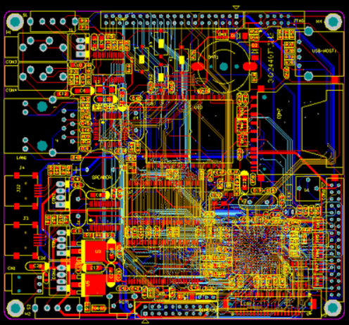
PCB design is more than putting together a few components and drawing traces linking them together. While working on a PCB layout must be accorded to capturing the design specification and translating it into functional schematics. PCBs come in a variety of designs, so it is important to have a thorough understanding of the design process. Some of the key elements to consider when designing a PCB include:
*Application for which the PCB will be used
*Environment in which the PCB will operate
*Amount of space and configuration required for installation
*Flexibility of the PCB
*Installation and assembly
Selecting the right PCB design to suit these considerations significantly impacts manufacturability, production speed, product yield, operation costs, and lead times.
PCB layout and design steps:
Create the Schematic
Create a Blank PCB Layout
Schematic Capture: Linking to Your PCB
Designing Your PCB Stackup
Defining Design Rules and DFM Requirements
Place Components
Insert Drill Holes
Route Traces
Add Labels and Identifiers
Generate Design Files
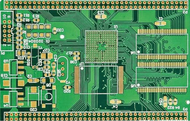
Printed Circuit Board Manufacturing
PCB manufacturing is the process that transforms a circuit board design into a physical structure based upon the specifications provided in the design package. Mainly achieved through the following steps or techniques:
- Imaging desired layout on copper clad laminates
- Substrate board preparation, the base material often comes in a large piece. We need cut it into designed size, and clean the surface of board in order to get the circuit pattern of good quality.
- Etching or removing excess copper from inner layers to reveal traces and pads
- Layup and lamination press
- Drilling holes for mounting holes, through hole pins and vias
- Plating pin holes and via holes
- Solder mask application to protect the circuit in the following soldering step, we need a protective coating to surface, or called solder mask
- Surface treatment, HASL (hot air solder leveling) or ENIG (electroless nickel immersion gold) to help ensuring the soldering quality of solder pad and to prevent oxidation
- Silkscreen printing reference and polarity indicators, logos or other markings on the surface
- Optionally, a finish may be added to copper areas of surface
- Do a sequence of test and then pack the board.
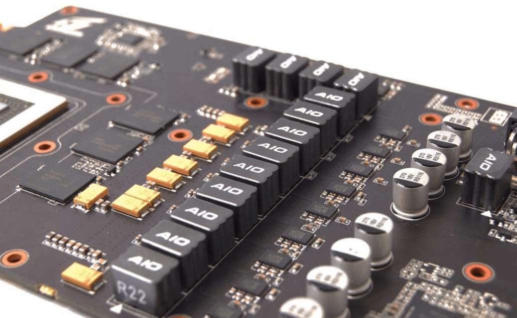
PCB Assembly and Production Process
Within a printed circuit board electronics assembly / production or manufacturing process there are a number of individual stages. However it is necessary for them all to work together to form an integrated overall process. Each stage of assembly and production must be compatible with the next, and there must be feedback from the output to the input to ensure that the highest quality is maintained. In this way any problems are detected quickly and the process can be adjusted accordingly.
1 – Application of Solder Paste
This is the very first step of a PCB assembly. Solder paste is applied to the board with the help of a solder screen. The screen has small holes. It is placed on the board at the correct position and a runner is moved across it. This allows the solder paste to squeeze through the holes and get applied on the board.
2.Placement of the Components
This is done after the application of solder paste. Surface Mount Technology (SMT) requires precise placement of components, components are placed on the board with the help of a pick and place machine.
3.Reflow Oven
After the component placement, the circuit board is placed on the reflow oven conveyor belt. The solder applied during the solder paste process melts during the reflow soldering. This joins the components to the circuit board permanently.
4.Inspection
After the reflow process, the PCB is subjected to inspection to check for its functionality. This stage helps identify poor quality connections, misplaced components, and shorts due to the consecutive movement of the board during the reflow process. The PCB manufacturers employ several inspection steps such as Visual Inspection, automatic optical inspection, and X-ray inspection to examine the functionality of the board, recognize lower-quality solder, and identify any potentially hidden problems.
5.Through-Hole Component Insertion
Some types of PCBs require the insertion of through-hole components in conjunction with the usual SMD components. This stage is devoted for such component insertion. For this, plated-through hole is created with the help of which PCB components pass signals from one side of the board to the other. The PCB through-hole insertion usually Manual Soldering or Wave Soldering to achieve the results.
6.Wave Soldering
In this step, the printed circuit board is placed on a mechanical conveyor driven system and passed through different zones. The PCB is passed over a molten solder wave, which helps connect the PCB pads/holes, electronic component leads, and the solder.
7.Final Inspection and Functional Test/ IC Programming
After the soldering step of the PCBA process is finished, a final inspection will test the PCB for its functionality. This inspection is known as a “functional test”. The test puts the PCB through its paces, simulating the normal circumstances in which the PCB will operate. Power and simulated signals run through the PCB in this test while testers monitor the PCB’s electrical characteristics.
8.Cleaning and Packing
As the soldering process leaves some amount of flux residues in PCBs, it is crucial to clean the assembly thoroughly before shipping the final board to a customer. For this, the PCBs are washed in deionized water. After the cleaning process, the board is dried thoroughly utilizing compressed air. The PCB assembly is now ready for the customers’ check and inspection.
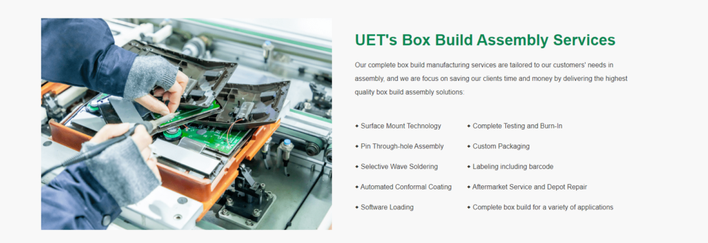
Box Build Assembly
Box build assembly is an electromechanical assembly process, which involves fabrication of enclosures, installation of cables or wire harnesses, and installation of components and sub-assemblies.
Box Build Assembly Process
Sub-Level Product Assembly
Design and engineering for mechanical components (injection molding, die casting, etc.)
Enclosure Fabrication,
installation of components and sub-assemblies
Routing of Cabling or Wire Harnesses,
System Level Assembly
Software Loading and Product Configuration
Functional Testing
Complete Product Testing & Burn-In
Custom testing systems with integrated software and hardware solutions.
Packaging & Labeling
Warehousing, Order Fulfillment, and Traceability
Custom tooling and fixtures
Build-to-order and configure-to-order (BTO & CTO)
Direct shipment to point of sale
Full turnkey solution