
USB is one of the most common terms heard now and then in the modern world of technological innovation. It is the USB that has all our data, which charges the devices we use, and which we can carry with us anywhere we go.
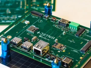
One of the most important things is understanding that USB is not just about the connection it creates. The main component through which it can perform so well is the PCB that is present within it.
USB PCB is responsible for carrying out all the functions for which we use it, including storing data, charging our devices, and ensuring appropriate data transfer.
In this guide below, we have featured many details about USB PCB that you might be looking forward to, so let’s read below.
What is USB PCB?
The first thing is making yourself aware of what a USB PCB is; it is a circuit board comprising a USB connector. This connector helps transfer data between devices and hence plays an essential role for all the gadgets we use around us.
The performance of these PCBs transfers data associated with high performance, thermal management, and controlling of the devices.
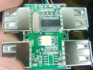
USB PCBs are not just used as connections. They also help in backing up the file and folders, which are essential, and allowing the programs to be accessed through wireless networks. The USB hub PCB is also present in multiple other equipment like those used in the medical and industrial sectors.
Essential Components in the USB PCB Design
The USB hub PCB has an exceptional design comprising some of the essential components, which are discussed below, as each has its functions.
1. Shielding
Shielding is the covering that acts as protection leading to preserving the PCB. This protection is needed because it could be damaging if the signal part is exposed to loud sound. Hence, adding a shielding saves the signal part from damage.
2. Stable Power Connections
The USB hub PCB comprises stable power connections, letting the connection between the data cords take place. It comprises power pins on the connector, ensuring that the device is resisted from powering above the data lines that could damage the USB.
3. Polarization
Polarization ensures that every USB has a one-sided orientation because connecting it from different sides may lead to damage. Hence, a USB needs to be connected in just one direction.
4. Strain Relief
It is important to have a plastic coating on the USB, as it is known as strain relief. This coating helps protect the USB from the tension that may be caused in the electrical link and leads to damaging it.
5. Four Contacts
The design of a USB comprises four contacts, and some USB 3.0 hub PCB may comprise more than four contacts, and these contacts tend to serve the power. The power served is through ground data lines.
Pros and Cons of USB PCB
As everything has some pros and cons similarly, the USB on PCB also has some pros and cons, which are shared below:
Pros of USB PCB
- USB PCBs allow versatile connectivity between devices and hence allow transferring data between different kinds of devices and charging them.
- The speed of transferring data using a USB is breakneck, and this is because the PCB it has supports this speed. Compared to other kinds of USBs, the USB PCB 3.0 and the USB PCB 3.1 are much faster.
- USBs can do multiple tasks at a time because of the functionality offered by the PCBs; they can transfer data and charge the device simultaneously. As long as the smartphones or tables are connected to the power source, for instance, a laptop, they will keep charging.
- USB PCBS supports a straightforward and quick functionality that works with the plug-and-play method allowing devices to function efficiently without complex processes.
Cons of USB PCB
- There is always a security threat to these USB PCs because they are susceptible to catching malware and viruses, which may damage the data in the devices.
- The length of the USB cable may be manageable, and hence it causes a limitation to portability because a longer length disrupts the transfer of data.
- The USB PCB connectors are susceptible to mechanical stress because they do not possess a very robust design. Hence, they need to be handled very carefully.
Reasons for USB PCB Failure
USB PCBs may fail and cause a problem in working, and many reasons lead to such failure, some of which are discussed below:
- Temperature change is one of the reasons that impact the PCB working, and it causes the dielectric material to be harmed. Therefore, the USB may stop working the way it should.
- If the device is drawing excessive power or the power circuitry has a problem, there could be a voltage drop, device failures, and noise in the power supply.
- USBs may get damaged due to the electrostatic discharge, and this kind of damage is permanent; hence, to avoid this, the design must have ESD protection devices.
- Sometimes the PCB has some manufacturing defects like components faults or traces are missing, which also leads to causing a failure in the USB interface.
- Mechanical stress is intolerable for most USBs; hence, if subjected to it, there might be a loss of connection that leads to the USB being completely damaged.
- Signal problems also lead to a problem with the USB, possibly due to the lack of proper routing or issues with the interface. It causes data transfer to get slow, and the entire data may be lost.
- The USB interfaces must be compatible with the other USB devices to be used simultaneously. If the PCB doesn’t support this compatibility, there could be severe problems with usability.
After going through the guide above, you must have learned a lot of things about the USB PCB and its significant role in USBs. Whether it is the USB connector or the USB that stores data, both must be backed with a good-quality PCB to ensure that it functions without any faults.