Defect Analysis and Process Improvement of BGA Solder Joints

We will discusses the acceptance criteria, defect performance and reliability of BGA solder joints. In particular, a more thorough analysis is carried out on a controversial defect-void. We also propose some process improvements to improve the quality of BGA solder joints.

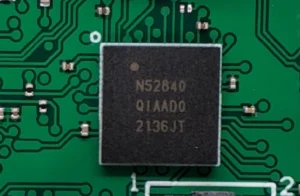
1. Introduction to BGA


BGA is a ball grid Chen packaged device. It appeared in the early 1990s. At that time, due to the increasing number of device pins in leaded packages, the lead spacing became smaller and smaller, resulting in the smallest device spacing reaching 0.3mm (12mil). For assembly, this has reached the limit in terms of manufacturability and reliability of device soldering. This will lead to an increased chance of error. At this time, a new type of ball grid array package device appeared. Compared with QFP devices of the same size, BGA can provide up to several times the number of pins.
For BGA, the solder balls under the chip are equivalent to the pins. The pitch of the pins is relatively large, which is a good thing for assembly. Can greatly improve the welding qualification rate and first-time success rate.


The PBGA, which is usually packaged in plastic, is the most widely used device in communication products and consumer products. Its solder ball composition is common 63n/37Pb, eutectic solder. CBGA devices in ceramic packages are sometimes used in military products, and its solder balls are a high-temperature 10Pb/90 Sn non-eutectic solder. With the continuous development of BGA devices, the United States and Japan have developed miniature BGAs with smaller packages, whose package size is only 20% larger than the chip.

Generally called μBGA (microBGA) or CSP. Their solder balls have reached a minimum of 0.3mm (12mil), and the solder ball spacing has reached a minimum of 0.5mm (12mil). In fact, for printed board manufacturers, making vias between such a small solder ball pitch is an important task. Very difficult job.

bga_pcb

2. Inspection of BGA soldering quality


Inspecting BGA soldering quality is challenging due to the solder balls being underneath the chip. Without inspection equipment, visually check if the outermost soldering ring is consistent and inspect the chip against light. If every row and column can transmit light, then it can be concluded that there is no continuous welding. Sometimes the solder with a larger size can also be seen. In order to judge the quality of solder joints more clearly, an X-RAY inspection instrument must also be used.
Traditional two-dimensional X-ray direct radiography equipment is relatively cheap. However, it has a drawback. Solder joints on both sides of the PCB are developed simultaneously in one photo. When components are present on both sides at the same position, their solder shadows overlap. This makes it difficult to distinguish the component’s side. If there is a defect, it is not clear which layer is the problem. Thus, the requirement of accurately determining welding defects cannot be met.
Our X-ray circuit board inspector is an X-ray tomographic inspection equipment specially used to inspect solder joints. Of course, it can not only check BGA, but also check the solder joints of all packages on the circuit board. Although it was previously thought that such equipment was too expensive, the cost of inspecting solder joints was too high. But with the application of BGA devices more and more widely, people have been able to accept this expensive equipment.
X-Ray uses X-ray tomography. Through it, the solder balls can be layered, creating a tomographic effect. X-ray tomography images can be used to automatically analyze solder joints based on CDA original design data and user-set parameters. It performs tomographic scanning in real time, and can accurately compare and analyze all solder joints of all components on both sides of the PCB within tens of seconds or 2 minutes (depending on the number and complexity of solder joints on the circuit board). Draw the conclusion of whether the welding is qualified or not. Why can X-ray photography of tomography obtain very high-definition results? This is determined by its working principle.
The X-rays of the X-ray system are generated by an X-ray tube located at the upper end of the device. When working, the voltage must be raised from 220V to 160KV, and the current is 100mA. Electron beams generated at high voltages irradiate metal tungsten to generate X-rays. This beam of X-rays shoots down obliquely and rotates at a high speed of 760 revolutions per second. At the same time, a scintillator platform below also rotates synchronously with the X-ray at the same speed.

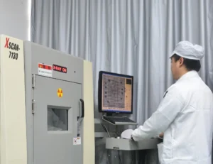
The scintillator platform is actually an X-ray sensitive receiver. Generally speaking, metals, heavy metals such as tin and lead will not pass through X-rays, and will form a dark scene. Ordinary matter is penetrated by X-rays, and nothing can be seen. The X-rays are gathered at a certain position between the light source and the scintillator platform, and a gathering plane appears. Objects or images on the focusing plane form a sharp image on the scintillator platform. But objects or images that are not on the gathering plane are blurred on the scintillator platform, leaving only a shadow.


The principle of X-ray judgment tomography is shown in the figure. Therefore, tomography is performed on solder joints with different heights on the PCB. If you want to check the soldering condition of a certain layer, you only need to adjust this layer to the position of the gathering plane, and the scanning results will be displayed clearly. This clear picture will be taken by an X-ray camera under the device.

pcb_bga

3. Acceptance criteria for BGA solder joints

No matter which inspection equipment is used for inspection, there must be a basis for judging whether the quality of solder joints is qualified. IPC-A-610C specifically defines the acceptance criteria for BGA solder joints. The requirements of the preferred BGA solder joints are that the solder joints are smooth, round, with clear boundaries and no voids. The diameter, volume, gray scale and contrast of all solder joints are the same, the position is aligned, there is no offset or twist, and there is no solder ball.
After completion, the preferred standard is pursued, but slightly relaxed for qualified solder joints. For aligned positions, the BGA solder joint can have an offset of no more than 25% relative to the pad. The solder ball should not exceed 25% of the distance between the nearest solder balls.

4. Typical defects of BGA solder joints

Typical defects of BGA include: solder joints, open circuits, missing solder balls, large voids, large solder balls, and fuzzy edges of solder joints. The following is a list of X-ray photographs encountered in actual work, including most of the above-mentioned defects.

5. A controversial defect – void

One issue that is still in dispute is the acceptance criteria for voids in BGAs. The void problem is not unique to BGAs. Solder joints for through-hole and surface-mount and through-hole components can usually be visually inspected for voids rather than x-rays. In BGAs, since all solder joints are hidden under the package, they can only be inspected by X-rays. Of course, X-rays can be used to inspect not only BGA solder joints, but also all kinds of solder joints. Using X-rays, voids can be easily detected.
So the void must have a negative impact on the reliability of the BGA? uncertain. Some even say that voiding is good for reliability. The IPC-7095 standard, titled ‘Design and Assembly Process for Realizing BGA,’ provides detailed guidelines for BGA design and assembly technology. The IPC-7095 committee acknowledges that small, unavoidable voids may be beneficial for reliability. However, there should be a defined standard to determine the acceptable size of voids.

5.1 The position and cause of the void

Where can voids be found in BGA solder joint inspection? BGA solder balls can be divided into three layers, one is the component layer (substrate close to the BGA component), one is the pad layer (substrate close to the PCB), and the other is the middle layer of the solder ball. Depending on the circumstances, voiding can occur in any of these three layers.
When did the void appear? BGA solder balls may themselves have voids in them prior to soldering, thus forming voids after the reflow soldering process is complete. This may be due to the introduction of voids in the solder ball manufacturing process, or the problem of the solder paste material coated on the PCB surface. In addition, the design of the circuit board is also a main reason for the formation of voids.
For example, if the via hole is designed under the pad, during the soldering process, the outside air enters the molten solder ball through the via hole, and a cavity will be left in the solder ball after the soldering is completed and cooled.
The voids in the pad layer may be due to the volatilization of the flux in the solder paste printed on the pad during the reflow soldering process, the gas escapes from the solder in the deep penetration, and the voids are formed after cooling. Poor pad plating or contamination on the pad surface may be the cause of voids in the pad layer.
The component layer is often the area with the highest likelihood of voids, located between the solder ball center and the BGA substrate. This could be due to air bubbles and volatilized flux gas on the BGA pad during reflow soldering on the PCB. Hollow is formed when united. If the reflow temperature curve is not long enough in the reflow zone, the air bubbles and the volatilized gas in the flux have no time to escape, and the molten solder fry has entered the cooling zone and becomes solid, forming a cavity.
Therefore, the reflow temperature profile is a cause of void formation. The BGA of eutectic solder 63n/37Pb is most likely to have voids, and the BGA composed of 10Sn/90Pb illegal eutectic high-melting point solder balls has a melting point of 302°C and generally has no voids. The solder balls on the BGA do not melt during the flow soldering process.

5.2 Void acceptance criteria

The presence of gas in the cavity may cause stress of shrinkage and expansion during thermal cycling. The location of the cavity will become a stress concentration point and may become the root cause of stress cracks.
However, the presence of voids reduces the mechanical stress on the solder balls by reducing the excess space applied by the solder balls. The specific reduction depends on the size, location, shape and other factors of the cavity.
The acceptance/rejection criteria for voids specified in IPC-7095 mainly consider two points: the position and size of voids. No matter where the void exists, whether it is in the middle of the solder ball or in the pad layer or component layer, depending on the size and quantity of the void, it will affect the quality and reliability. Small solder balls are allowed inside the solder balls. The ratio of the space occupied by the void to the space of the solder ball can be calculated as follows: for example, the diameter of the void is 50% of the diameter of the solder ball, then the area occupied by the void is 25% of the area of the solder ball.
The IPC standard specifies that voids in the pad layer should not exceed 10% of the solder ball area. Voids exceeding 25% are considered defects, posing risks to mechanical and electrical reliability. For voids between 10% and 25%, process improvement is recommended to eliminate or reduce them.

6. Conclusion Suggestions for process improvement to reduce BGA defects

When the BGA of eutectic solder forms solder joints during the soldering process, the solder paste coated on the PCB and the solder balls contained in the components must be fused together. This process is divided into two stages of collapse. The first stage of collapse is that the solder paste on the PCB melts first, and the components collapse. In the second stage, the solder balls of the components themselves also melt and fuse with the melted solder paste on the PCB, and the solder balls again Collapsing, forming an oblate solder joint.

To form a perfect solder joint, the following aspects should be paid attention to:

(1) Use fresh solder paste to ensure that the solder paste is evenly stirred, the position of the solder paste coating is accurate, and the position of the component is accurate.


(2) For plastic packaged PBGA, it should be dried at 100°C for 6-8 hours before soldering, and it is better if there is nitrogen.


(3) The reflow temperature profile is a very important factor.

During the welding process, it is necessary to ensure that the welding curve transitions naturally, so that the device is evenly heated, especially in the

welding area, it is necessary to ensure that all solder joints are fully melted. If the temperature is insufficient, cold solder joints may form, causing rough solder joint surfaces or incomplete melting during the second slump stage. This can lead to cracks between the solder paste on the PCB surface and the component’s solder, resulting in virtual or open soldering.

(4) The amount of solder paste applied must be appropriate.

The solder paste’s viscosity helps temporarily secure the device and prevent solder bridging during melting. For BGA templates, the solder joint opening is typically 70-80% of the pad size, and the template thickness is usually 0.15mm (6mil).


(5) When designing the pads of BGA on the PCB, the pads of all solder joints must be designed to be the same size.

If some processes must be designed under the pads, you should also find a suitable PCB manufacturer. The pad position should be drilled, and unauthorized enlargement of the pad should be avoided. This is because the via hole cannot be drilled too small. As a result, the amount of tin and the height will differ after soldering between the large and small pads. Weld or open circuit.


(6) In addition, one point should be emphasized about the solder mask problem during PCB production.

Before soldering a BGA, ensure the solder mask around the pad is qualified and vias are coated with a barrier film. Adding solder resist film on the other side of the PCB during production is ineffective. The purpose of solder resist film is to prevent air and void formation during soldering, as well as to prevent solder flow through through holes.


Printing solder paste without rework avoids excess solder and improves soldering quality. Via holes are plated, so excess solder or soldering issues can cause virtual short defects and short circuits. BGA rework is a last resort because it takes a long time.

Conclusion

To solder BGA successfully, we need suitable solder balls and rework tools. Ball planting has low success rates and wastes resources. Repaired chips endure at least 4 reflow cycles, affecting reliability. Prepare well before soldering BGA to minimize defects and achieve a high pass rate. Our goal is to eliminate defects without repairing.

Leave a Reply

Your email address will not be published. Required fields are marked *