
PCBs are a fundamental part of the design process in the electronic industry, and this article will provide you with an overview of what they are and how they differ from other types of circuit boards. PCBs can be utilized for prototyping, fabrication, and manufacturing purposes, but understanding all these pcb manufacturing process is important to make sure that your project goes smoothly.
PCB prototyping
When you’re developing a new electronic product or component. It’s crucial to know that the completed item will function as expected, this is why it’s an industry standard to create a PCB prototype. Computer modelling can help, but until you hold a functioning model in your hands, you won’t have a real sense of performance.
Making a prototype PCB is the first opportunity to get your design in person. This is your chance to iron out any design flaws, increase the material allocation, and impress stakeholders or investors with an interest in your project before moving on to volume or batch manufacturing.
Hi5 Electronics has years of expertise transforming concepts and PCB layouts into working prototypes. We’d be delighted to do the same for yours.
PCB fabrication
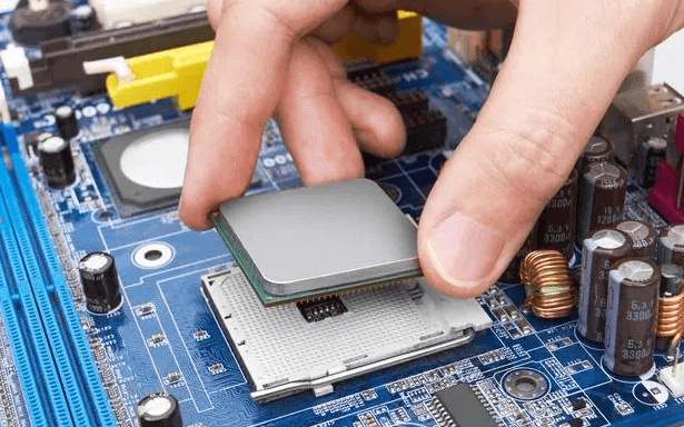
PCB fabrication is the process of putting together printed circuit boards (PCBs). The board’s surface pattern is linked with the required layers, allowing it to be utilized in electronics production. PCBs may be created internally by third-party experts or outsourced to PCB Chinese manufacturing companies.
Customers can also develop their own files and send them to the manufacturer for the PCB fabrication using a format known as a Gerber file. This is an industry-standard for recording the specification of a cheap PCB manufacturing process.
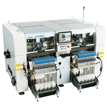
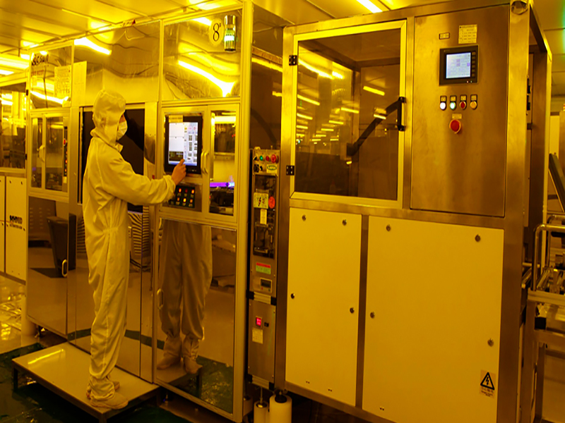
PCB Manufacturing Process
The Design
You need a drawing of your board before you start the PCB manufacturing process. Computer software is often used to design circuits on the computer. Trace width calculators are the best way to get information about layers inside and outside.
Printing the design
A plotted printer is used to print the board’s design. In the PCB Manufacturing Process, It generates a film that displays the card’s intricacies and layers. There will be two ink colors on the board’s inner layer when it is produced.
Creating the substrate
The printed films are cut into layers. In the PCB Manufacturing Process,the insulating material made with epoxy resin and glass fiber is put through a machine to be semi-cured or heated. One side of the layer is pre-bonded with copper before being cut away to reveal the design from the printed film.
Printing the Inner layers
The design is printed to a laminate, which serves as the structure’s body. The resist film, composed of photo-reactive chemicals that will solidify when exposed to UV light, covers the board. This can be used to align the blueprints and print. Holes are drilled into the PCB for use in alignment.
Ultraviolet light
The resist and laminate are exposed to ultraviolet radiation, which hardens the photoresist, after they have been properly aligned. The pathways of copper are revealed by the light. The dark ink from before inhibits the formation of a solid barrier in regions that will be removed later on.
Laminating the Layers
Construction is now in full swing. In the PCB Manufacturing Process,you can see how it progresses as the layers are put together. The laminating process starts with metal clamps holding the layers together. A prepreg (epoxy resin) layer is applied to the alignment basin. Then a substrate layer is added, followed by a copper foil layer.
Pressing the Layers
A machine is used to press the layers together. Pins are put in between the layers, which keep them in place. The pins can be removed depending on what type of technology is being used. If it is correct, then the PCB goes to the laminating machine where heat and pressure are applied to fuse all of the layers together.
Drilling
To reveal the substrate and inner panels, holes are drilled through the layers using a computer-controlled drill. Any remaining copper is subsequently removed after this phase.
Plating
The board is now ready to be put on the plate. In the PCB Manufacturing Process, a solution that we make fuses all of the layers together. After that, we wash it and give it a thin copper coating in the holes.
Outer Layer Imaging
When the outside layer is completed, it’s coated with a coat of photoresist that’s similar to Step 3. In the PCB Manufacturing Process,the photoresist is hardened using ultraviolet light. Any unwanted photoresist is eliminated.
Plating
The panel is plated with a thin copper layer, just as it was in Step 11. A tiny tin guard is then added to the board. The tin is used to prevent the outer layer’s copper from being eroded by acid.
Etching
The same chemical solution used before removes any unwanted copper under the resist layer. The tin guard layer protects the needed copper. This step set up the PCB’s connections.
Solder Mask Application
Clean the panels before you put on the solder mask. In the PCB Manufacturing Process,the solder masks are put on with a liquid called epoxy. When the solder mask is baked on. It will give your board a green color. You can remove unwanted solder masks with ultraviolet light while you keep what you want by baking them in the oven for a certain period of time.
Silkscreening
Silkscreening is a process that prints words on the board. The board then goes through another process called coating and curing.
Surface Finish
Depending on the demands, PCB Manufacturing Process is plated with a solderable finish, which improves the quality and bond of the solder.
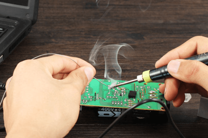
Testing
Before the PCB is finished, a technician will test it to make sure it works. This should be done before any other steps are taken.
This PCB Manufacturing Process is usually expensive with most suppliers however cheap PCB manufacturing is often found with PCB Chinese companies.
Why is PCB Prototyping Important?
In the PCB Manufacturing Process, having a PCB prototype is essential. It’s possible that a major design flaw might be discovered in the middle of production, and it can be costly to fix. Not to mention how difficult this change would be. Therefore having a PCB prototype is a must-do to stop any potential issues when producing at scale.
You can dramatically improve the performance of your final product by improving the efficiency of your design during prototyping. In the PCB Manufacturing Process, you may also correct any flaws that might have an impact on the quality or efficacy of your finished product this way.
Design engineers like to test single PCB prototype boards or functions separately with more complicated goods that have several features and PCBs. Using a prototype allows them to try out simple features before adding more layers of intricacy. This not only helps enhance specific capabilities, but it can also aid in the isolation and identification of problems later on in the design PCB Manufacturing Process.