
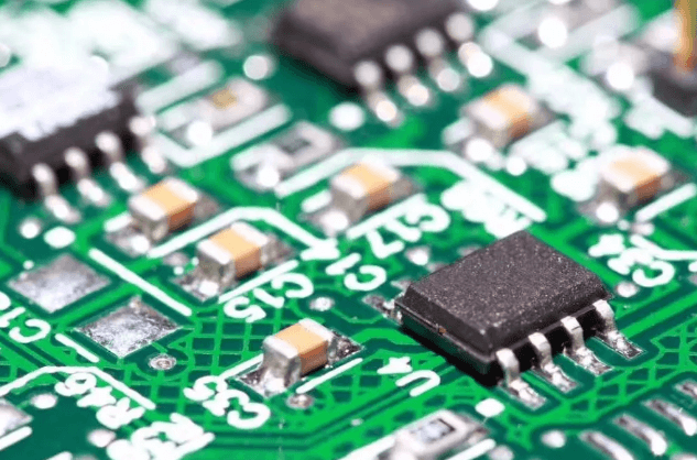
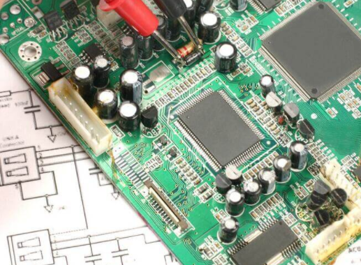
PCBs are used in a wide range of electronic devices, including computers, smartphones, and other digital equipment. They have become ubiquitous because they offer high reliability at a low cost. However, there are many different ways to treat the surface of a PCB before it is assembled with other components into an electronic device. Which one should you choose? This guide will provide information on three common PCB surface finishes: OSP (organic solderability preservative), HASL (hot air solder leveling), and ENIG (electroless nickel immersion gold).
Why is PCB surface finishes important?
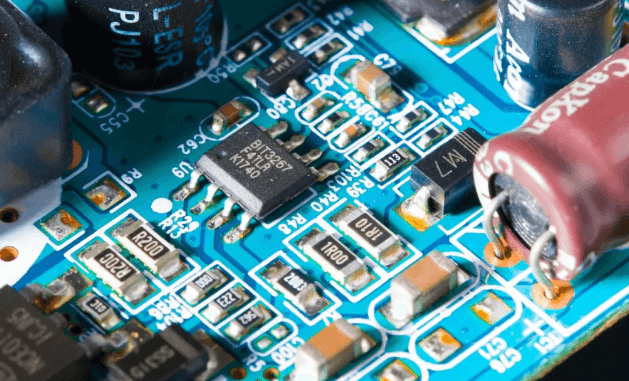
The PCB surface finishes are an important interface between the component and the PCB. The finish’s two primary functions are to shield the exposed copper wiring and to offer a solderable surface for joining (soldering) the components to the printed circuit board.
What is pcb surface finishes?
The process of applying a PCB surface layer to the PCB is known as PCB surface finishes. The objective of PCB surface finishes are to guarantee that the PCB has good solderability and electrical properties. There are numerous varieties of printed circuit board surface treatments available. PCB Surface treatment is a multistage process that includes the following steps:
- Chemical treatment of chemical etching or electropolishing
- Organic coating followed by baking at high temperature
- Cationic electroless nickel plating and chemical conversion to Ni/Sn surface alloy
- Anodic aluminium oxide (Al-oxide) coating
- Organic coating followed by baking at high temperature as in step C.
What is OSP?
Copper is continuously oxidized by the air, which leaves it discoloured and brittle. Anti-oxidation preserves the pcb surface finishes from corrosion by forming a very thin protective layer of material over the exposed copper, usually on a conveyorized system.
It’s made of a water-based organic compound that binds to copper and creates an organometallic layer that protects the copper before soldering. It is also far more environmentally friendly than standard lead-free finishes, which are either more hazardous or require considerably more energy use.
Advantages and Disadvantages of OSP
Advantages
Lead-free
OCB is a lead-free process so it is more environmentally friendly than the traditional HASL.
Cost
OSP can treat pcb surface finishes at a much lower cost. This is because it requires less material to soak and rinse when the pcb surface finishes. This also reduces waste disposal costs. If you are already using a lead-free solder paste (which has a lower volume than standard solder pastes)
Flat pcb surface finishes
OSP has a very flat pcb surface finishes, which can be beneficial when working with components that have tight tolerances. The smoothness of the HASL finish may cause issues in this case because it is more likely to pick up debris from the air and trap solder paste.
Simple process
OSP offers a simple PCB Surface Finishes process, which makes it much easier to maintain and control each board’s quality. This is an advantage if you need large quantities or have very tight tolerances. OSP handles PCB Surface Finishes as minor inconsistencies in solder masks can cause problems.
Repairable
The OSP process is repairable, which means that if you damage the finish on the board. Or if you need to remove it to fix a soldering problem. There is a way to remove it and replace it without having to throw away the whole PCB.
Disadvantages
Limited to RoHS compliance
OSP is only compliant for materials that are free from lead, cadmium and mercury. This means it cannot be used with any non-RoHS components or boards made of other types of metals. For this reason, OSP can’t replace both HASL and ENIG in all situations.
Environmental impact
Although OSP is a lead-free process, it requires the use of solvents that have their own environmental impacts which need to be taken into consideration. The cleaning steps also produce wastewater. So there may still be concerns about its effect on the environment if large volumes are required.
Sensitive
OSP is sensitive to the effects of heat over time.This means that it may need a rework process if boards are located in areas with higher temperatures. This can mean additional costs and resources for your business.
Short shelf life
OSP is a water-based finish, which means it has a limited shelf life. It’s typically only good for around two months if left in an open container and can be ruined by exposure to humidity or moisture over time.
What is HASL?
The majority of pcb surface finishes are finished with HASL, which stands for hot acid pickle wash. The method entails submerging circuitry boards in a molten tin/lead alloy and then removing the extra solder using ‘air knives,’ which blast hot air across the pcb surface finishes. HASL is often available lead-free which is an advantage on its own.
The HASL method, by virtue of its extreme heat treatment, exposes the PCB to temperatures up on lowest initial wet adhesion than other finishes, it has the 265°C, allowing for the detection of any delamination concerns prior to the use of costly components.
Advantages and Disadvantages of HASL
Advantages
Low-cost
HASL is a low-cost process that can be completed quickly and easily. The method requires fewer steps than other pcb surface finishes making it ideal for the lower volume applications required by many components manufacturers, particularly in smaller production runs. HASL is often available lead-free which is an advantage on its own.
Repairable
HASL offers minimal protection to your circuitry board’s copper base. However, if damage occurs after the HASL process is completed, it can be fixed quickly and easily.
Lead free
HASL is available in lead-free versions, which are compliant with the RoHS directive. This means that it can be used for all types of components including those made from non-RoHS materials or metals, unlike OSP options. HASL lead-free is free from lead, cadmium and mercury.
Simple process
HASL offers a simple production methodology that’s ideal for smaller volumes or where tight tolerances are required. The simplicity of the method makes it easy to control quality levels which means you don’t have to worry about variations in solder thickness across different boards.
Available in multiple finishes
HASL is available in several different grades, each with its own benefits. Pure Tin/Lead has the lowest melting point of 269°C but also requires more cleaning steps to remove excess material after soldering. HASL Sn-Cu offers a higher melting point of 227°C. This means there are fewer chances for delamination. HASL with ENIG offers the highest soldering temperatures, which makes it ideal for high-reliability applications.
Disadvantages
Short shelf life
HASL has a short shelf life of around six months in an open container due to its exposure to humidity and moisture over time. It’s particularly sensitive to this after each step in the soldering process.
Environmental impact
HASL is a lead-based finish which means it’s not compliant with all environmental standards, particularly those that are based on RoHS compliance as HASL doesn’t meet these requirements without additional plating processes. This can result in customers refusing to buy products from you if they’re unwilling to take the risk of potential non-compliance issues.
Lead exposure
HASL is a lead-based finish which means it’s not compliant with all environmental standards, particularly those that are based on RoHS compliance as HASL doesn’t meet these requirements without additional plating processes. This can result in customers refusing to buy products from you if they’re unwilling to take the risk of potential non-compliance issues.
Thermal Shock
HASL produces the most thermal shock of any surface finish, which means it is more susceptible to delamination. The combination of the chemicals used in the process requires high temperatures during soldering and also results in a hot board that can be cooled down quickly with water or air.
Poor Wetting
HASL has poor wetting properties, which means it’s not suitable for use with aluminium or other non-ferrous metals. This can increase the cost and complexity of your designs because you’ll need to consider how different materials interact during soldering operations.
What is ENIG?
GOLF METAL is a pcb surface finishes that combines the corrosion resistance of anodized aluminum with the polish and shine of natural metal. It features a nickel shell over a copper underlayer, which acts as both a barrier to protect against oxidation and a solder target for components to bond to. During storage, a layer of gold is applied to the nickel. ENIG is a solution to big industry trends such as lead-free regulations. The rise of complicated surface components (particularly BGAs and flip chips), which necessitates flat surfaces.
It is worth noting that ZENIG does not protect against corrosion due to ionic-based attacks. In most cases, this type of alloy will require more frequent cleaning and maintenance than many metals because of the difficulty in maintaining a moisture barrier between the gold and nickel layers.
Advantages and Disadvantages of ENIG
Advantages
Flat surfaces
ENIG offers a level of flatness that can be beneficial for components with tight tolerances. The smooth pcb surface finishes may also help to prevent issues in this case due to the high risk of trapping solder paste on HASL boards, which has been proven by experiments at Stanford University and MIT.
Long-lasting
When it comes to protecting PCBs from corrosion, ENIG offers a significant advantage over other surface treatments as the gold layer is extremely thin and will not require rework or replacement, unlike traditional anodizing techniques that can wear off after extensive use. The performance of ENIG also increases over time as adhesion builds up between the nickel and gold layers.
ENIG’s gold layer provides increased adhesion for components, which makes it ideal if you’re using parts that are sensitive to heat or have low melting points. The extra solder can also help with thermal management issues during reflow soldering processes, as the use of ENIG will reduce warpage caused by excess heating time compared to HASL.
Lead-free
ENIG is lead-free compatible, which means it can be used for projects that are subject to RoHS compliance. This may help you avoid additional costs. Especially if your components or circuit boards require expensive rework in order to meet environmental laws.
Good for PTH
As ENIG is a thick, flat material that can be used en-masse for an entire board, it makes the process of plating through holes more cost-effective.
Maintains solderability during storage
ENIG’s resistance to moisture means components are less likely to corrode or delaminate while stored in humid conditions prior to use. This can boost quality and consistency across your production circuit boards. This means you have more time to focus on other aspects of the design process. Without having to worry about potentially costly errors caused by water damage.
Disadvantages
Flammable
If a PCB is not designed properly, ENIG may expose layers that are flammable or that may release toxic fumes. This is why it is important to have your PCBs inspected by a professional before use.
Weaker bond for components
ENIG’s gold layer can be thinner than other pcb surface finishes. This means less solder will build up around the component pads. This reduces thermal management issues during reflow soldering processes. Components are more likely to fall off boards or become loose after being soldered.
Requires professional installation
ENIG is a pcb surface finishes that requires advanced training and expertise in order for it to be applied correctly. This means you cannot install ENIG yourself. This can lead to additional costs if your PCBs require expensive rework because of quality issues.
Requires special materials
ENIG requires the use of gold plated nickel and can be expensive to replace if it wears down over time. It also requires the use of a special cleaner in order for boards to maintain their corrosion resistance. After they’ve been soldered, which may add some additional costs to your production process.
Why do we need pcb surface finishes?
Solderability
The ability of a metal or alloy to form a solid connection with solder. A soldered joint is formed by first applying a thin layer of liquid paste (flux) over the area where two metallic surfaces will be joined. Then placing very small pieces of solder on the paste. When heated, the liquid paste melts and covers the surfaces being joined with a thin layer of molten solder. That can flow into any areas where there are irregularities in either surface or between two surfaces.
Surface Finish
A material’s physical characteristics are beyond its chemical composition. For example, most metals have certain colors associated with them, such as silver or gold. Therefore, surface finish is an important factor in determining the appearance of a metal object.
High reliability at a low cost
This is key to pcb surface finishes as it provides a better connection between the component and the PCB. This is what you want for your electronic devices. As it will last longer and be more effective than an uncoated or poorly treated board.