
For decades, printed circuit board assembly (PCBA) has successfully developed in a stable manner. It is a key component of various machines, computing terminals, automobiles and other electronic equipment. It is compact and efficient. In addition, they electronically introduce new inventions and technologies on a global scale. They have set off an innovation in the electronics industry.
The method of circuit board identification
1.Resistance – Circuit board identification
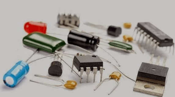
Use “R” plus a number in the circuit to represent the resistance, such as: R1 represents the resistance numbered 1. The main functions of resistors in the circuit are: shunting, current limiting, voltage division, biasing and so on. Parameter circuit board identification: The unit of resistance is ohm (Q2), and the multiplication unit is: kiloohm (KQ), megohm (MQ2), etc
2. Capacitance – Printed circuit board parts identification
Generally use “C” plus a number in the circuit (for example, C13 represents the capacitor numbered 13) to represent Capacitors. A capacitor is a component composed of two metal films close together and separated by an insulating material in the middle. The characteristic of the capacitor is mainly to block the direct current and pass the alternating current. The size of the capacitor capacity is the size that can store electrical energy. Calling the obstructive effect of the capacitor on the AC signal capacitive reactance, which is related to the frequency and capacitance of the AC signal.
Circuit board components identification method: The circuit board identification method of capacitance is basically the same as that of resistance, divide it into three types: direct labeling method, color labeling method and numerical labeling method.
3.inductance
Usually use “L” plus a number in the circuit to represent inductance. such as: L6 represents the inductance numbered 6. By winding an insulated wire around a certain number of turns on an insulated frame to make the inductance coil. DC can pass through the coil, and the DC resistance is the resistance of the wire itself, and the voltage drop is very small; When an AC signal passes through the coil, the two ends of the coil will automatically generate self-induced electromotive force. The direction of the self-induced electromotive force is opposite to the direction of the applied voltage, which hinders AC Pass, so the characteristic of the inductance is to pass DC and resist AC, the higher the frequency, the greater the coil impedance. Inductance and capacitance can form an oscillating circuit in a circuit.
Inductance generally has direct calibration method and color calibration method, and the color calibration method is similar to resistance. For example, brown, black, gold, and gold represent an inductance of 1uH (error 5%). The basic unit of inductance is: Hen (H) The conversion unit is: 1H=103mH=106uH.
4. Crystal diode
Circuit board component identification usually use “D” plus a number in the circuit to represent crystal diodes. Such as: D5 represents the number 5 diode. The main characteristic of the diode is unidirectional conductivity, that is, under the action of forward voltage, the on-resistance is very small; and under the action of reverse voltage, the on-resistance is extremely large or infinite. Because the diode has the above-mentioned characteristics, often use it in circuits such as rectification, isolation, voltage stabilization, polarity protection, pcb identification code control, frequency modulation, and noise suppression in cordless phones.
Circuit board components identificationmethod: The circuit board parts identification of diodes is very simple. Mostly mark the N pole (cathode) of low-power diodes with a color circle on the outside of the diode. Some diodes also use a special symbol for the diode to indicate the P pole (positive diodes also use special symbols for the diode To indicate P pole (positive) or N pole (negative), there are also mark symbols as “P” and “N” to determine the polarity of the diode. The positive and negative poles of the light-emitting diode can be identified by the length of the pin, and the long leg is positive , The short foot is negative.
5.crystal triode
Circuit board parts identification usually use “Q'” plus a number in the circuit to present transistor, such as: Q17 represents the number of 17 transistor .The crystal triode (triode for short) contains two PN junctions inside and is a special device with amplification capability. Divide it into two types: NPN type and PNP type. These two types of transistors can make up for each other in terms of working characteristics. The so-called pair of transistors in OTL circuits is paired with PNP type and NPN type.
6.Zener diode
Identification circuit board components often use “ZD’ plus numbers in the circuit to present zener diodes. Such as: ZD5 represents the Zener tube numbered 5. The principle of voltage stabilization of Zener diodes: The characteristic of Zener diodes is that the voltage at both ends of the Zener diode is basically maintained after breakdown. No change. In this way, when the voltage regulator tube is connected to the circuit, if the voltage of each point in the circuit fluctuates due to fluctuations in the power supply voltage or other reasons, the voltage at both ends of the load will basically remain unchanged.
Fault characteristics: The fault of the Zener diode is mainly manifested in open circuit, short circuit and unstable voltage regulation value. Among these three types of failures, the former type of failures show an increase in the power supply voltage; the latter two types of failures show that the supply voltage drops to zero volts or the output is unstable.
7.varactor diode
The varactor diode is a special diode specially designed based on the principle that the junction capacitance of the internal “PN junction” of the ordinary diode can change with the change of the applied reverse voltage. Varactor diodes are mainly used in the high-frequency modulation circuit of mobile phones or landlines in cordless telephones to achieve modulation of low-frequency signals to high-frequency signals and transmit them.
In the working state, the modulation voltage of the varactor diode is generally added to the negative electrode, so that the internal junction capacitance of the varactor diode changes with the change of the modulation voltage.
How to circuit board components identification
The first step to pcb component identification:
First determine the printed circuit board. Usually this is a basic rectangular chip or circuit board, usually green or blue.
The second step to circuit board parts identification:
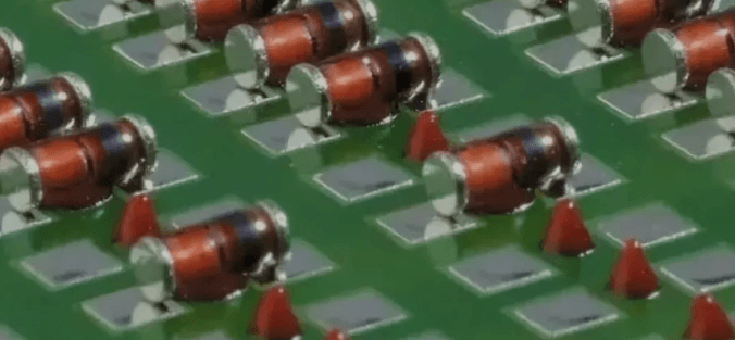
Identify other types of circuit board components. Generally these components control and adjust the current of the entire power board. Including resistance: color code tube to reduce current. Capacitors and potentiometers: usually rectangular or circular, and use ohm variable resistance to measure the mark. Oscillator: When mark the cylinder or box with “X” or “Y”. Electrical box (marked with the letter “K”) and transformer (marked with a “T”). And other electronic components such as passive components (with two bifurcated wires) and sensors (spiral pieces).
The third step to circuit board components identification:
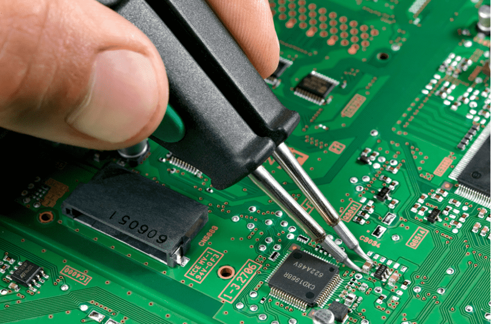
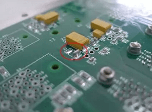
Locate the battery, fuse, diode, and transistor of the circuit board. The battery is a small tube, similar to the appearance of a small household battery. Similarly, the fuse fuse may resemble your home fuse. Diodes are connected to wires (they are usually marked with “D”) and look like transparent or translucent tubes. Transistors are small pieces and thin metal connections.
The fourth step to identify circuit board parts:
Find the processor. They are usually small squares or rectangles in computer circuit boards. In some cases, the central processing unit (CPU) may be marked with the company’s name. In addition, sometimes to prevent overheating, a small electric fan can be placed under the processor.
The fifth step to identify circuit board parts:
Look for the motherboard circuit board. Designers may sometimes attach small circuit boards (especially motherboards) to other places, such as rectangular slots. So, the connector wires will be very long, especially the connection between the boards.
The sixth Step to identify circuit board parts:
Find other chips on the circuit board. Usually print these smaller chips on the silicon board under other components.
The seventh Step to identify circuit board parts:
Please find the RAM (Random Access Memory) connected to the circuit board. A circuit board may be like a small gray box, and the supplementary RAM is an elongated rectangular chip.
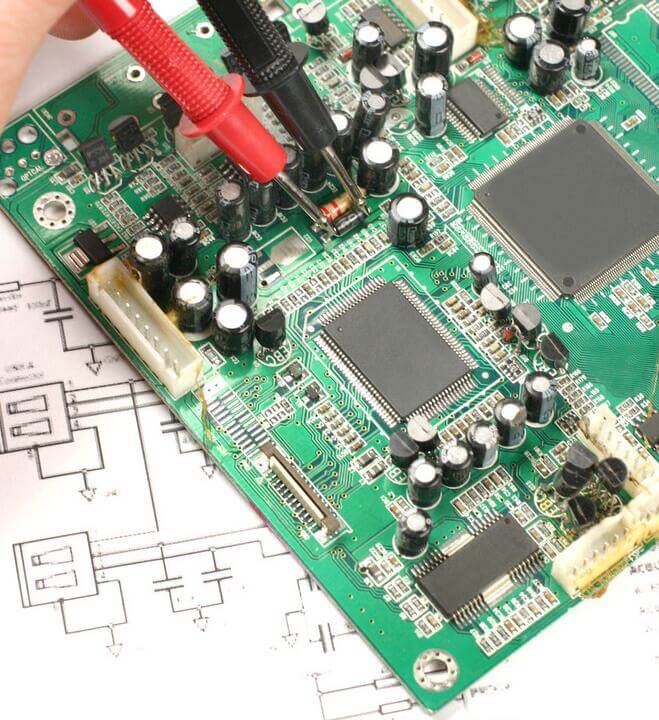
How to assemble circuit board components
Before using a fully operable electronic device, connecting the electronic component to the printed circuit board is the end action.In short, the process of a printed circuit board assembly is the wiring connection between the electronic assembly and the printed circuit board. Traces or conductive paths are engraved on the laminated copper plate of the PCB for non-conductive substrates to form components. And It must be noted that the assembly of the circuit board is different from the manufacture of the circuit board. Manufacturing printed circuit boards involves multiple processes, including PCB design and creating PCB prototypes. After preparing the PCB, solder the electronic components to it. Only then can it be applied to electronic devices or gadgets. The method of assembling electronic components depends on the circuit board, the type of electronic components and the purpose of the circuit board. But the general steps are similar.
Solder paste printing:
solder paste printing is the basic step of PCBA circuit board assembly. Although there are many types of PCB assembly, this step is applicable to all types. Placing a steel mesh made of a thin metal plate on the plate. Do this to ensure that the solder paste is only in the area where installed the components. Then apply solder paste on the stencil and remove it from the board.
Pick and place component installation:
Use an automated system instead can perform component installation manually or mechanically. Usually in the through-hole PCB assembly, it will perform manually the system. In the assembly activities of surface mount PCBs, automated machines perform operations. Automatic component installation provides a fast, accurate and error-free process.
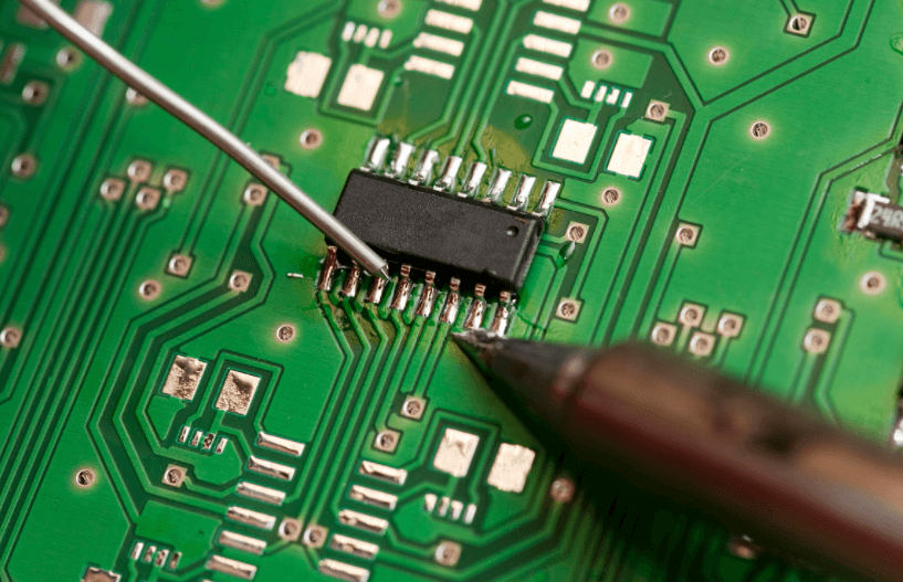
Soldering:
Performing soldering to connect the components on the PCB.Use wave soldering when in the execution of through-hole component activities. In this case, the PCB with the components installed will move on the hot wave soldering fluid. This will liquefy the solder balls and then cool them at room temperature to solidify the solder paste. In addition, when PCB components are mounted on the surface, use reflow soldering to perform them. In this case, it is by placing the PCB in a furnace heated to a temperature of 500°F. This way the solder paste will melt and settle with the component when it cools.
Inspection:
Carry out inspection and quality test to ensure that the function of the equipment can operate normally. It involves three different inspection methods, as described below. There are many forms.
- The first type, appearance/manual inspection: manual inspection is only suitable for inspecting solder connections. Usually use this method when inspecting small batches of PCBs.
- The second, automatic optical inspection (AOI): The high-resolution camera of the AOI machine can point the machine at different angles to test the PCB. Optical inspection can only meet single or double size PCB inspection, but it is not suitable for multi-layer complex PCB inspection.
- The third type, X-ray inspection: when performing complex PCB designs with multi-layer component mounting apply X-ray inspection. Such complex PCBs are difficult to inspect optically.