
what is a printed circuit board?
Introduction:
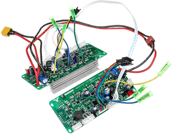
The printed circuit board comprises an insulating bottom plate, connecting wires and pads for assembling and welding electronic components. And It has the dual functions of conductive lines and insulating bottom plates. Integrated circuits and electronic components such as resistors and capacitors cannot function as a single individual. Only when they have a foothold on the printed circuit board and have a conductive junction to connect them can they perform their functions in this whole. The printed circuit board is the skeleton that supports the components and the pipeline that connects the electrical signals. Some printed circuit boards have ingredients such as resistors, capacitors, and inductors attached to them, which become functional circuits and act as devices.
Influences:
Printed circuit boards are the basis of electronic equipment. This is to say, the circuit boards make the circuit miniaturized and intuitive and play an essential role in the mass production of fixed courses and optimizing electrical appliances’ layout. Because the various components in place are selected, they connect to do the electronic equipment work as expected. It can replace complex wiring and realize the electrical connection between the various components in the circuit. And,it simplifies the assembly and welding of electronic products, traditionally reduces the workload of wiring, dramatically reduces the labour intensity of workers, reduces the overall machine Volume, reduces product cost, and improves the quality and reliability of electronic equipment.
Expand:
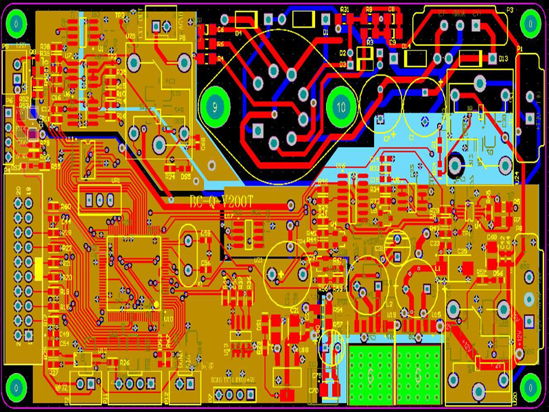
The printed board’s technical level is a sign of double-side and multi-hole metallize printed boards: it is a double-side metallized printed board produced in large quantities. At the intersection between the pads, the 2.50 or 2.54mm standard grid, it can be laid the number of wires as a sign. It laid a wire between the two residences and placed a low-density printed board with a wire width greater than 0.3mm on the wire. Arrange two wires between the two pads. This is a medium-density printed circuit board with a wire width of about 0.2mm. We placed three wires between the two houses, which is a high-density printed circuit board. And the wire width is about 0.10-0.15mm. Arrange four wires between the two pads, regard it as an ultra-high-density printed board with a line width of 0.05-0.08mm.
What is the circuit board made of?
The material of the circuit board
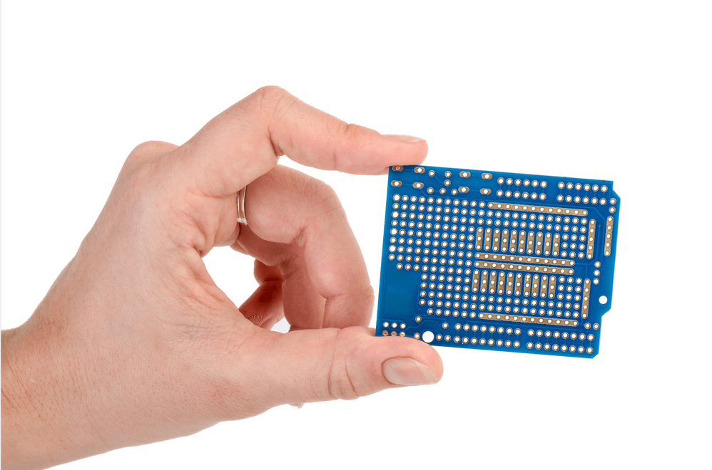
The printed circuit board (PCB) ‘s primary material is copper-clad laminate, and the compose is a substrate, copper foil, and adhesive. Firstly, the substrate is an insulating layer board. It’s written are synthetic polymer resin and reinforced materials; Cover the substrate’s surface with a layer of pure copper foil with high conductivity and good solderability. The usual thickness is 35-50/ma, cover the copper foil on the substrate. Secondly, the copper-clad laminate on one side which called single-sided copper-clad laminate. And the copper-clad laminate with copper foil on both sides of the substrate called double-sided copper-clad laminate; Generally, the adhesive complete whether could firmly cover the copper foil on the substrate. Commonly used copper-clad laminates have three thicknesses: 1.0 mm, 1.5 mm and 2.0 mm.
The circuit board has become the most active industry in the modern electronic component industry. And its industry growth rate is generally about three percentage points higher than that of the electronic component industry. And in recent years, with the development of the electronics industry, the market demand for circuit boards increases. Therefore, there are also many types of copper-clad laminates. Different insulating materials can be divided into paper substrate, glass cloth substrate, and synthetic fiberboard. Similarly, according to various binder resins, it can be divided into phenolic, epoxy, polyester and polytetrafluoroethylene; it can be divided into the general type and particular type according to the purpose.
The structure and characteristics of commonly used copper clad laminates
- Copper clad phenolic paper laminate
A laminate made of insulating impregnated paper (TFS-62) or cotton fibre impregnated paper (1TZ-63) impregnated with phenolic resin and then hot pressed. In conclusion, with a single sheet of alkali-free glass impregnated cloth that can attach the adhesive tape on both surfaces. Cover one side with copper foil. Mainly use it as a printed circuit board in radio equipment.
- Copper clad phenolic glass cloth laminate
It is a laminate made of alkali-free glass cloth impregnated with phenolic epoxy resin and hot pressed. One or both sides of it has a copper foil. It has the advantages of a lightweight, good electrical and mechanical properties, and convenient processing. The surface of the board is light yellow. If using melamine as the curing agent, the board’s surface is light green and has good transparency.
- Copper clad PTFE laminate
It is a copper-clad board with PTFE board as the substrate, covered with copper foil and hot-pressed. Mainly use it for printed boards in high frequency and ultra high-frequency circuits.
- Copper clad epoxy glass cloth laminate
It is a hole material metallized printed boards, usually use for hole metallized printed boards.
- Soft polyester copper-clad film
It is a ribbon-shaped material made of polyester film and copper by hot pressing. It is then rolled into a spiral shape and placed inside the device during application. In order to enhance or prevent moisture, we often pour it into a hole with epoxy resin. Besides, it is mainly used as a flexible printed circuit and printed cable and can use it as a transition line for connectors.
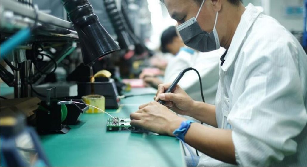
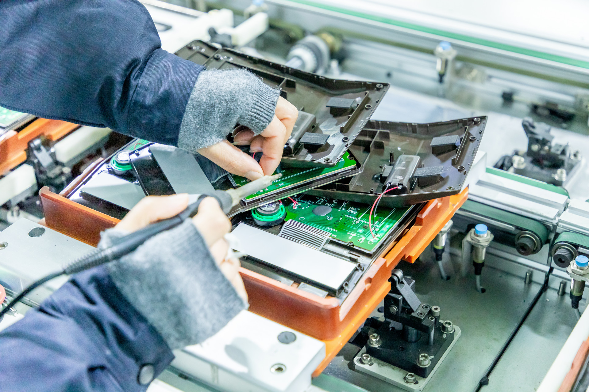
The Circuit board production process
1: Data optimization
The optimization of data directly relates to the ease of production, the utilization rate of materials; the scrap rate; the workload of the production line; So data optimization is the most critical core process in the board factory! Also, there is a big difference between the material optimization of the board factory and the friends of the project design project; it is necessary to understand the design data’s simple principles; communicate with the design project; prevent the product produced and the design requirements from inconsistency! Also, consider the typesetting design; this is closely related to the SMT factory’s work; a good typesetting design can help SMT save the situation of lousy placement; simultaneously, it can also increase the material utilization rate of the board factory!
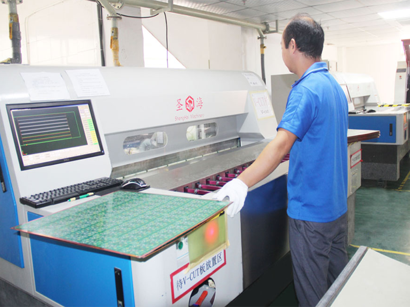
2: Cutting
From the engineering data to optimize the rule for cutting, the work board’s size and the material model of the project’s process are different. The size of the extensive material of each material model is different. There are usually two specifications for the available size: 41 *49. Therefore, if there are two material models of 43*49 inches, could divide it into many kinds. There are cardboard, fibreglass board, high-frequency board, high TG, etc.; manufacturers are also different. The most commonly used are Taiwan Nanya Jiantao Shengyi, PTFE and Rogers board, so please be sure to check the design project’s requirements.
3: Drilling
The primary purpose of drilling is to first connect the holes on the circuit board that need the plug-in to the via holes; Have fixed the required holes; Use the hole diameter is between 0.15-6.0 and can for CNC drilling; Only use the laser could to drill small holes (Note: The cost of this process is very high, and it is not recommended to use 0.1 Via holes in engineering design); the commonly used machines for drilling are currently Huaqiang machines and 48,84 system drilling machines; The drilling speed is between 160,000 and 200,000 revolutions; there are also 220,000 revolutions.
4: Immersion copper
Immersion copper means plating the drilled holes with copper. At present, there are two processes for sinking copper in China. Let’s come to the first one (1: Pure copper sinking process: This is the current old process and this can be satisfied.
The production of all circuit boards requires that the copper thickness of the hole can be more than 18um. The copper thickness of the gap can be more than 18um, and achieve the thickening of 30um to meet the requirements of the excessive current of the circuit board; the second is the blackening (conductive glue) process because the current price is cheap. The circuit board also can use the reason, but this process has a fatal flaw that the copper thickness of the hole wall is skinny, only between 12-16um. And it cannot pass the UL certification, and it cannot give high current and work for a long time).
5: Etching
The role of etching is to make the circuit board lines; the limit of etching is 2min usually 3min is suitable; the general board factory likes more than 5min; of course the more precise the higher the value.
6: Solder mask
This is to make a solder mask; the solder mask’s role is to discolour the corresponding colour and leak out where the window needs to be opened; the difficulty lies in the need to manufacture IC solder mask bridges BGAs on specific high-precision boards. IC solder mask bridges usually need to maintain a gap of 6 minutes between the bridges; the difficulty of BGA is that the BGA window is usually a little larger than the wire point and only about 1 minute on one side. It is not suitable for solder mask printing and poor alignment; If the window is too large, the resulting BGA points will not be round, and the window will be too large, resulting in solder slippage and defective products!
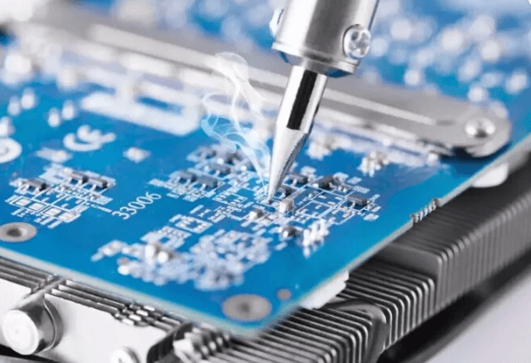
7: Character printing
There are three things to pay attention to when printing characters (the first is the colour and ink type; and the second is that the printing can not conflict with the pad to be printed on the place!)
8: Surface treatment
There are many processes for surface treatment. (commonly done are lead spray tin, lead-free tin spray, immersion gold, and electric gold, OSP, immersion tin, etc.)
9: Shape processing
There are two ways of shape processing: one is CNC; the other is die punching (CNC has a smooth appearance; mold punching is rough).
10: Test
Usually use test rack test and flying probe test are for testing; test rack test efficiency is much higher.
what is printed circuit board used for?
The function of the printed circuit board
PCB has the following functions in electronic equipment.
(1) Provide mechanical support for the fixing and assembly of various electronic components such as integrated circuits, realize the wiring and electrical connection or electrical insulation between various electronic components such as integrated circuits, and provide the required electrical characteristics.
(2) Provide solder mask graphics for automatic welding and identify characters and illustrations for component insertion, inspection, and maintenance.
(3) After electronic equipment adopts printed boards, manual wiring errors can be avoided due to the consistency of similar printed boards and automatically inserted or mounted electronic components, automatic soldering, and automatic detection, ensuring electronic products. The quality of the product improves labour productivity, reduces costs, and facilitates maintenance.
(4) Provide required electrical characteristics, characteristic impedance and electromagnetic compatibility characteristics for circuits in high-speed or high-frequency circuits.
(5) The printed circuit board with passive components embedded inside provides certain electrical functions, simplifies the electronic installation procedure, and improves the product’s reliability.
(6) In large-scale and ultra-large-scale electronic packaging components, provide an effective chip carrier for the miniaturized chip packaging of electronic components.
Features of printed circuit boards
The reason why PCB can be used more and more widely is that it has many unique advantages, which are rough as follows:
High-density
Over the years, the high density of printed boards has developed correspondingly with the improvement of integrated circuit integration and mounting technology advancement.
High reliability
Through a series of inspections, tests and ageing tests and other technical means, guarantee the PCB work reliably for a long time (usually 20 years).
Designability
Various properties of PCB can achieve the requirements (electrical, physical, chemical, mechanical, etc.) through design standardization and standardization. This way, the design time is short, and the efficiency is high.
Manufacturability
PCB adopts modern management, which can realize standardization, scale (quantity), and automatic production to ensure product quality consistency.
Testability
Have established a relatively complete test method and test standard by using various test equipment and instruments to detect and appraise PCB products’ eligibility and service life.
Assemblability
PCB products are convenient for standardized assembly of various components and automated and large-scale mass production. Besides, assembling the PCB and different other elements form more significant parts and systems to the complete machine.
Maintainability
Since assembling these PCB products and various components in a standardized design and large-scale production, so also standardize these components. Therefore, once the system fails, these can replace it quickly, conveniently and flexibly, and quickly restore the system to work.
PCB has other advantages, such as miniaturization and lightweight of the system, and high-speed signal transmission.