
PCB designers use digital design automation to generate a design frequently. The EDA app stores layout info, facilitates editing the plan, and automates repetitive design tasks.
The very first phase is converting the circuit schematic to a web list.
The web listing gives component hooks and the circuit structures or baits that every pin connects. The treaty catch the EDA application, operated by a circuit design engineer is in charge of netlist creation. In addition to this, we import netlist into the PCB design program is also necessary.
The next step is to determine the position of every apparatus.
define a grid of lettered rows and columns
The simple means is to define a grid of lettered rows and columns in which the appliance should proceed. The computer then assigns pin 1 of every device from the bill of materials to a grid location. Usually, the operator can help the automatic placement routine by defining rooms or particular circuit board areas. Then, we put specific groups of elements in it. The parts related to a power supply sub-circuit can connect to a region close to the power input. In other cases, you can position the apparatus manually. The maximize electric functioning of the circuit or even to put components is acceptable. The mechanical needs layout of this machine such as knobs, switches, and connectors.
The pc then explodes the apparatus list to an entire pin list to the circuit board. It will use templates from a library of footprints related to every kind of device. Each print is a map of a device’s hooks. Typically with a recommended pad and drill hole design for each apparatus. The library makes it possible for the footprint to be attracted just once. It will share with all devices of this type.
marking for attention from the Custom PCB designer
You can find the high-current pads in the machine library in specific systems and the affiliated baits marking for attention from the Custom PCB designer. High current runs demand broader traces, and also the trainee or circuit layout engineer usually determines the width.
The computer program then unifies the netlist (sorted by pin title) using the pinned listing (sorted by pin title), shifting the physical coordinates of this pin listing to the netlist. The netlist is then resorted by name.
Some systems may maximize the plan by adjusting the positions of components and logic gates to decrease the distance of copper runs. Some systems automatically find electricity hooks from the devices and create runs or vias to the closest power airplane or conductor.
track each net in the signal-pin listing
The applications then attempt to track each net in the signal-pin listing, locating some sequence of links in the available layers. Frequently layers are delegated to ground and power, with a single layer to vertical and yet another to horizontal wires. The electricity layers protect the circuits from the sound.
The navigation problem is equal to the traveling salesman problem and is NP-complete and therefore not amenable to some ideal answer. One functional routing algorithm selects the pin farthest from the middle of these circuit boards, then uses a greedy algorithm to choose the next-nearest pin with the same signal name.
After automatic routing, usually, there’s a record of nets that has to be manually routed.
decrease the manufacturing cost of the Custom PCB
After routed, the machine might have a streak of strategy subroutines to decrease the manufacturing cost of the Custom PCB. By way of instance, one routine may eliminate unnecessary vias (every vial is a drill hole, also costs money to create). Another may round borders of conductor runs and extend, or transfer runs apart to keep safe spacing. Another approach might fix large copper areas to shape nets, or extensive blank spaces may acquire unconnected “tests” of aluminum. The yields and tests decrease pollution by prolonging this whirlpool tub’s life span and accelerating production by evening-out the aluminum concentration in the whirlpool tub.
Some programs offer design rule checking to confirm the design for electric connectivity and clearance, guidelines for circuit board fabrication, construction and evaluation, heat flow, and other mistakes.
The silk-screen, solder mask, and solder paste stencil(s) are auxiliary layers.
get a structure of numerical control document to get a photoplotter
Eventually, we can convert the aluminum layers into Gerber files subsequently. And then, you can get a structure of numerical control document to get a photoplotter. Historically, an extra aperture file was obligated to connect each numerically specified aperture known at the Gerber file using a natural contour. You can decipher the natural shape, which embeds the aperture info in the Gerber file. The files include hole places. You can pile up the drill documents to minimize drill-head motion time and minor changes.
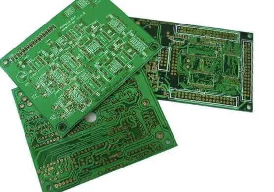
Physical makeup
Many PCBs include between one and sixteen (or more) reflective layers separated and supported by layers of insulating material (substrates) laminated (glued) together. Layers could be linked together through drilled holes called vias. You can electroplate the holes or insert the tiny rivets.
High-density PC might have blind vias, observable only on a single surface, or buried vias, which are visible on neither.